ZHCS509E
November 2011 – June 2018
OPA180
,
OPA2180
,
OPA4180
PRODUCTION DATA.
1
特性
2
应用范围
3
说明
低噪声 (峰值到峰值噪声 = 250nV)
4
修订历史记录
5
Device Comparison Table
6
Pin Configuration and Functions
Pin Functions
Pin Functions: OPA180
Pin Functions: OPA2180
Pin Functions: OPA4180
7
Specifications
7.1
Absolute Maximum Ratings
7.2
ESD Ratings
7.3
Recommended Operating Conditions
7.4
Thermal Information: OPA180
7.5
Thermal Information: OPA2180
7.6
Thermal Information: OPA4180
7.7
Electrical Characteristics: VS = ±2 V to ±18 V (VS = 4 V to 36 V)
7.8
Typical Characteristics: Table of Graphs
7.9
Typical Characteristics
8
Detailed Description
8.1
Overview
8.2
Functional Block Diagram
8.3
Feature Description
8.3.1
Operating Characteristics
8.3.2
EMI Rejection
8.3.3
Phase-Reversal Protection
8.3.4
Capacitive Load and Stability
8.3.5
Electrical Overstress
8.4
Device Functional Modes
9
Application and Implementation
9.1
Application Information
9.2
Typical Applications
9.2.1
Bipolar ±10-V Analog Output from a Unipolar Voltage Output DAC
9.2.1.1
Design Requirements
9.2.1.2
Detailed Design Procedure
9.2.1.2.1
Component Selection
9.2.1.3
Application Curves
9.2.2
Discrete INA + Attenuation
9.2.3
RTD Amplifier
10
Power Supply Recommendations
11
Layout
11.1
Layout Guidelines
11.2
Layout Example
12
器件和文档支持
12.1
相关链接
12.2
商标
12.3
静电放电警告
12.4
术语表
13
机械、封装和可订购信息
封装选项
机械数据 (封装 | 引脚)
D|8
MSOI002K
DGK|8
MPDS028E
散热焊盘机械数据 (封装 | 引脚)
订购信息
zhcs509e_oa
zhcs509e_pm
7.9
Typical Characteristics
V
S
= ±18 V, V
CM
= V
S
/ 2, R
LOAD
= 10 kΩ connected to V
S
/ 2, and C
L
= 100 pF, unless otherwise noted.
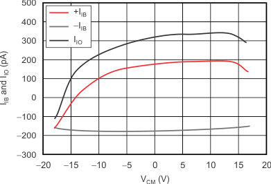
Figure 1.
I
IB
and I
IO
vs Common-Mode Voltage
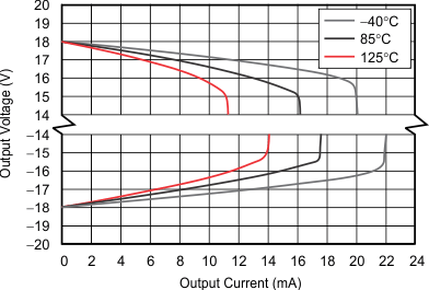
Figure 3.
Output Voltage Swing vs Output Current
(Maximum Supply)
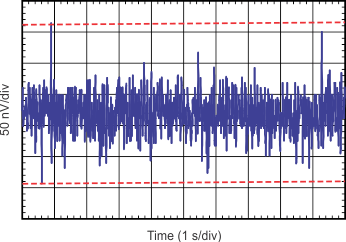
Peak-to-Peak Noise = 250 nV
Figure 5.
0.1-Hz to 10-Hz Noise
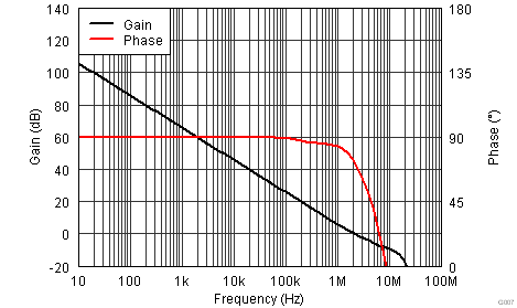
Figure 7.
Open-Loop Gain and Phase vs Frequency
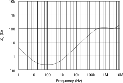
Figure 9.
Open-Loop Output Impedance vs Frequency
R
L
= 10 kΩ
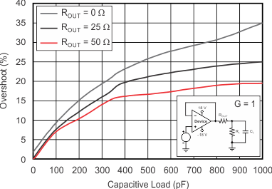
Figure 11.
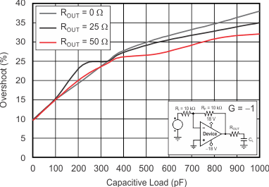
Small-Signal Overshoot vs Capacitive Load
(100-mV Output Step)
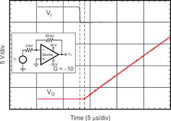
Figure 13.
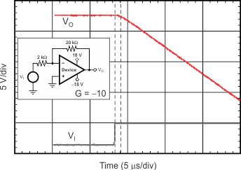
Positive Overload Recovery
R
L
= 10 kΩ
C
L
= 10 pF
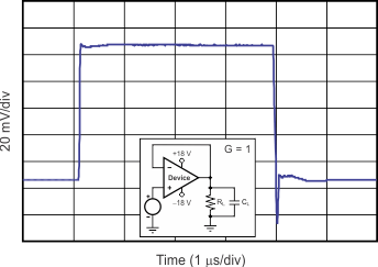
Figure 15.
Small-Signal Step Response
(100 mV)
G = 1
R
L
= 10 kΩ
C
L
= 10 pF
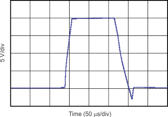
Figure 17.
Large-Signal Step Response
G = –1
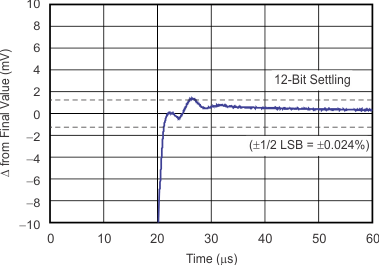
Figure 19.
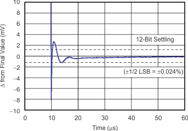
Large-Signal Settling Time (10-V Positive Step)
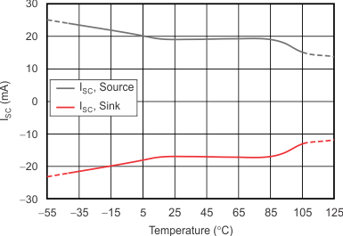
Figure 21.
Short-Circuit Current vs Temperature
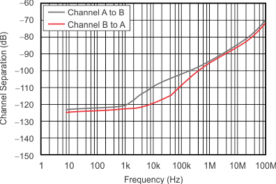
Figure 23.
Channel Separation vs Frequency
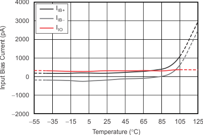
Figure 2.
Input Bias Current vs Temperature
V
SUPPLY
= ±2 V
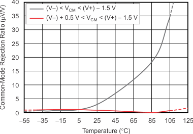
Figure 4.
CMRR vs Temperature
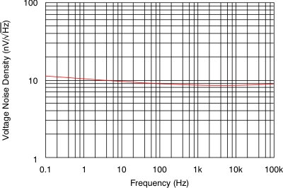
Figure 6.
Input Voltage Noise Spectral Density vs Frequency
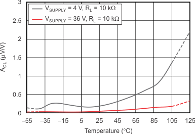
Figure 8.
Open-Loop Gain vs Temperature
R
L
= 10 kΩ
Figure 10.
Small-Signal Overshoot vs Capacitive Load
(100-mV Output Step)
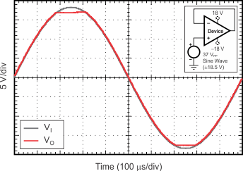
Figure 12.
No Phase Reversal
Figure 14.
Negative Overload Recovery
R
L
= 10 kΩ
C
L
= 10 pF
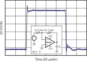
Figure 16.
Small-Signal Step Response (100 mV)
G = –1
R
L
= 10 kΩ
C
L
= 10 pF
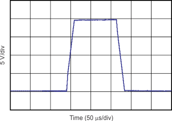
Figure 18.
Large-Signal Step Response
G = –1
Figure 20.
Large-Signal Settling Time (10-V Negative Step)
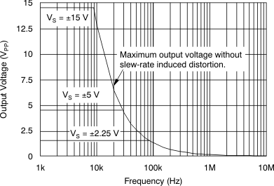
Figure 22.
Maximum Output Voltage vs Frequency
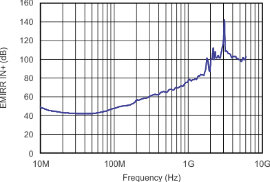
Figure 24.
EMIRR IN+ vs Frequency
千亿体育app官网登录(中国)官方网站IOS/安卓通用版/手机APP
|
米乐app下载官网(中国)|ios|Android/通用版APP最新版
|
米乐|米乐·M6(中国大陆)官方网站
|
千亿体育登陆地址
|
华体会体育(中国)HTH·官方网站
|
千赢qy国际_全站最新版千赢qy国际V6.2.14安卓/IOS下载
|
18新利网v1.2.5|中国官方网站
|
bob电竞真人(中国官网)安卓/ios苹果/电脑版【1.97.95版下载】
|
千亿体育app官方下载(中国)官方网站IOS/安卓/手机APP下载安装
|