SBOS850 December 2017 OPA192-Q1 , OPA2192-Q1
PRODUCTION DATA.
- 1 Features
- 2 Applications
- 3 Description
- 4 Revision History
- 5 Pin Configuration and Functions
-
6 Specifications
- 6.1 Absolute Maximum Ratings
- 6.2 ESD Ratings
- 6.3 Recommended Operating Conditions
- 6.4 Thermal Information: OPA192-Q1
- 6.5 Thermal Information: OPA2192-Q1
- 6.6 Electrical Characteristics: VS = ±4 V to ±18 V (VS = 8 V to 36 V)
- 6.7 Electrical Characteristics: VS = ±2.25 V to ±4 V (VS = 4.5 V to 8 V)
- 6.8 Typical Characteristics
- 6.9 Typical Characteristics
- 7 Parameter Measurement Information
- 8 Detailed Description
- 9 Application and Implementation
- 10Power-Supply Recommendations
- 11Layout
- 12Device and Documentation Support
- 13Mechanical, Packaging, and Orderable Information
7 Parameter Measurement Information
7.1 Input Offset Voltage Drift
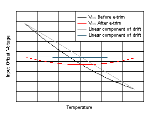
The OPAx192-Q1 family of operational amplifiers is manufactured using TI’s e-trim technology. Each amplifier input offset voltage and input offset voltage drift is trimmed in production, thereby minimizing errors associated with input offset voltage and input offset voltage drift. The e-trim technology is a TI proprietary method of trimming internal device parameters during either wafer probing or final testing. When trimming input offset voltage drift the systematic or linear drift error on each device is trimmed to zero. This results in the remaining errors associated with input offset drift are minimal and are the result from only nonlinear error sources. Figure 47 illustrates this concept.
 Figure 47. Input Offset Before and After Drift Trim
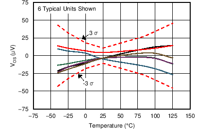
Figure 48 shows six typical units.
 Figure 48. Input Offset Voltage Drift vs Temperature for Six Typical Units