ZHCSLB1F april 2020 – march 2023 OPA205 , OPA2205 , OPA4205
PRODMIX
- 1 特性
- 2 应用
- 3 说明
- 4 Revision History
- 5 Pin Configuration and Functions
- 6 Specifications
- 7 Parameter Measurement Information
- 8 Detailed Description
- 9 Application and Implementation
- 10Device and Documentation Support
- 11Mechanical, Packaging, and Orderable Information
6.9 Typical Characteristics
at TA = 25°C, VS = ±15V, VCM = VOUT = midsupply, and RL = 10 kΩ (unless otherwise noted)
Table 6-1 Table of Graphs
| DESCRIPTION | FIGURE |
|---|---|
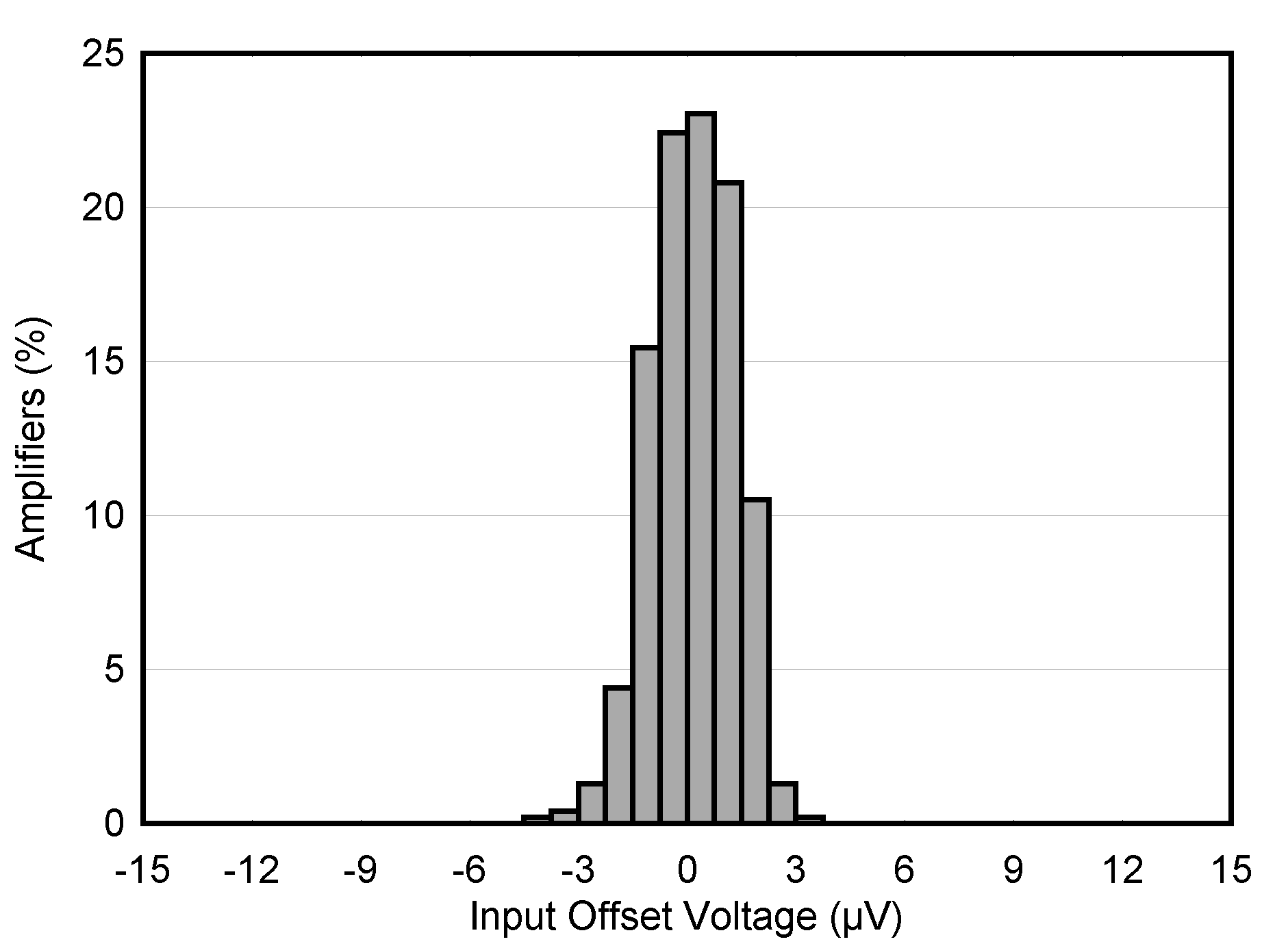
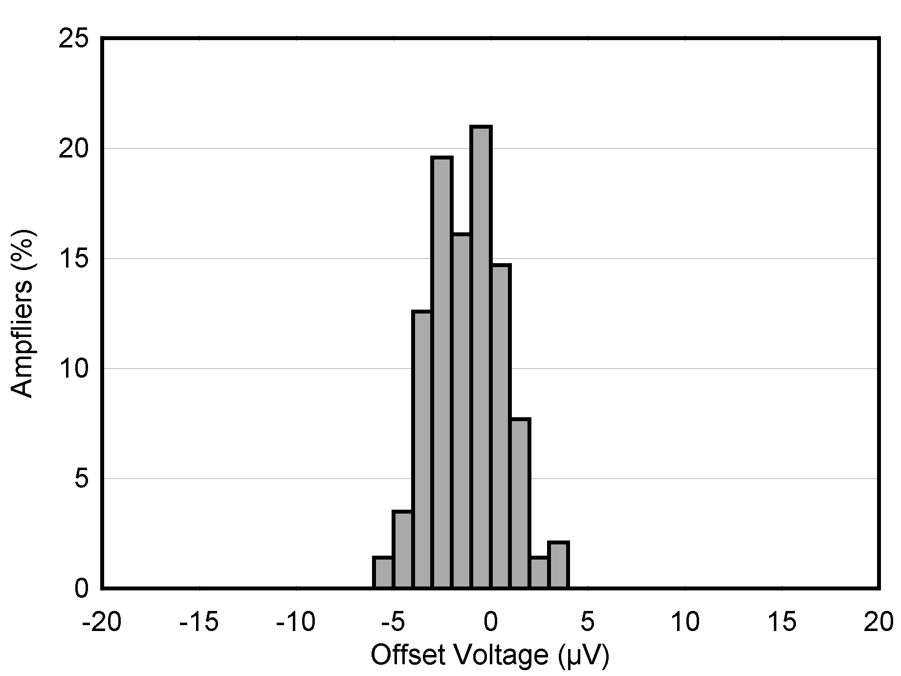
| Offset Voltage Production Distribution at 25°C | Figure 6-1 |
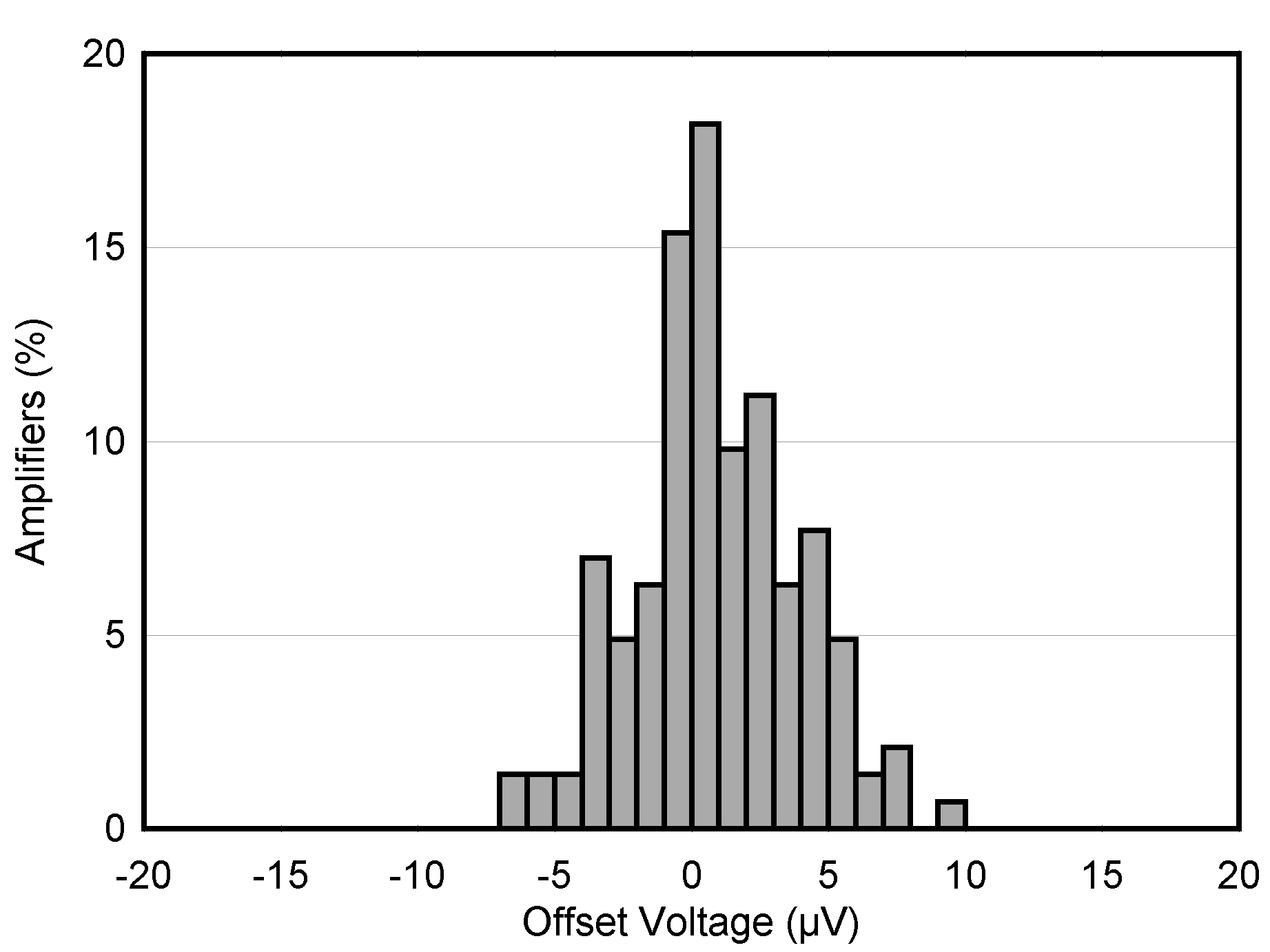
| Offset Voltage at 125°C | Figure 6-2 |
| Offset Voltage at –40°C | Figure 6-3 |
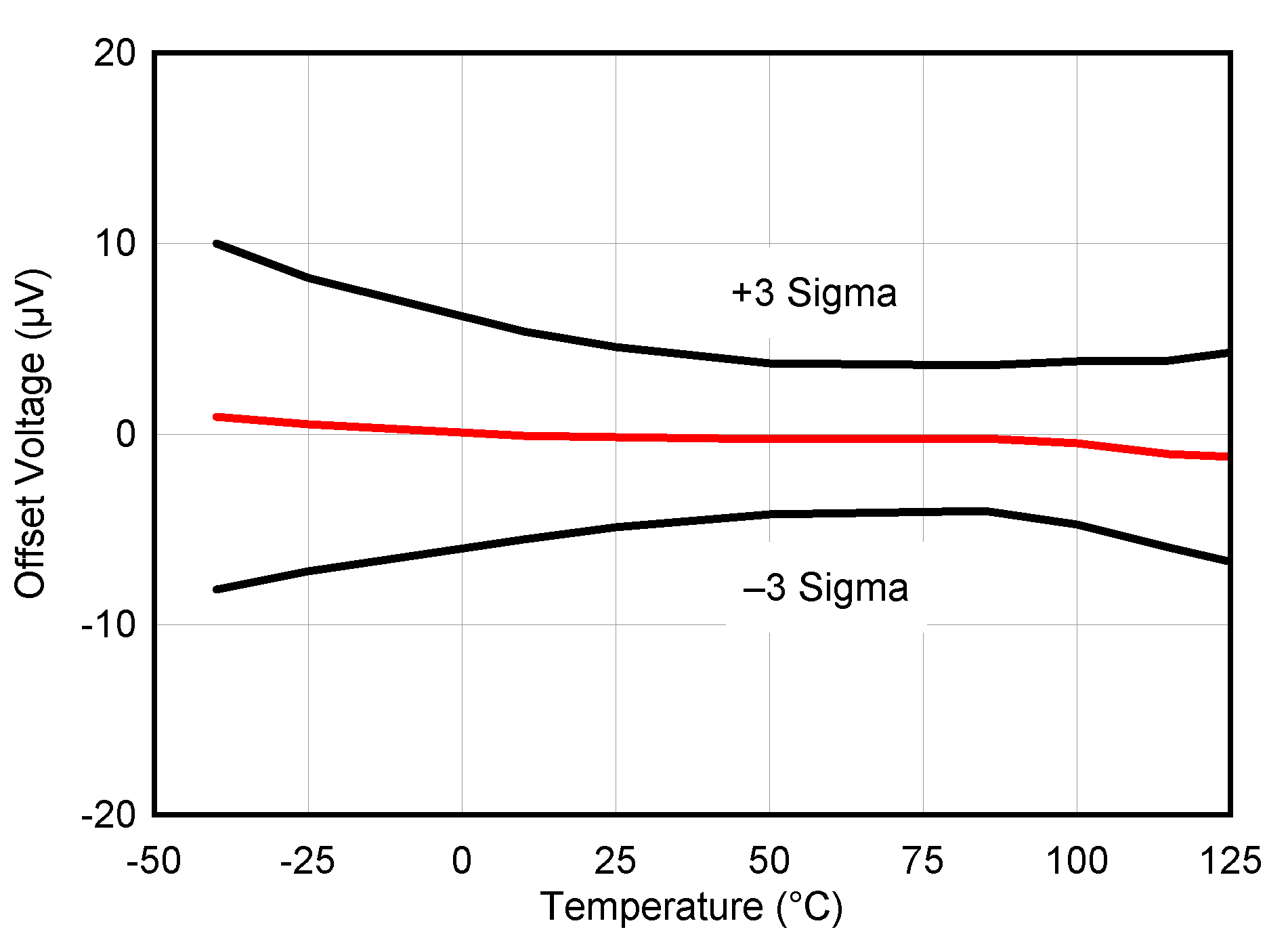
| Offset Voltage vs Temperature | Figure 6-4 |
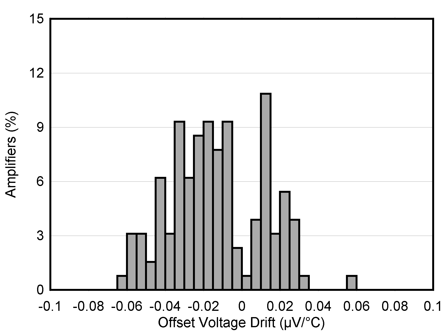
| Offset Voltage Drift Distribution | Figure 6-5 |
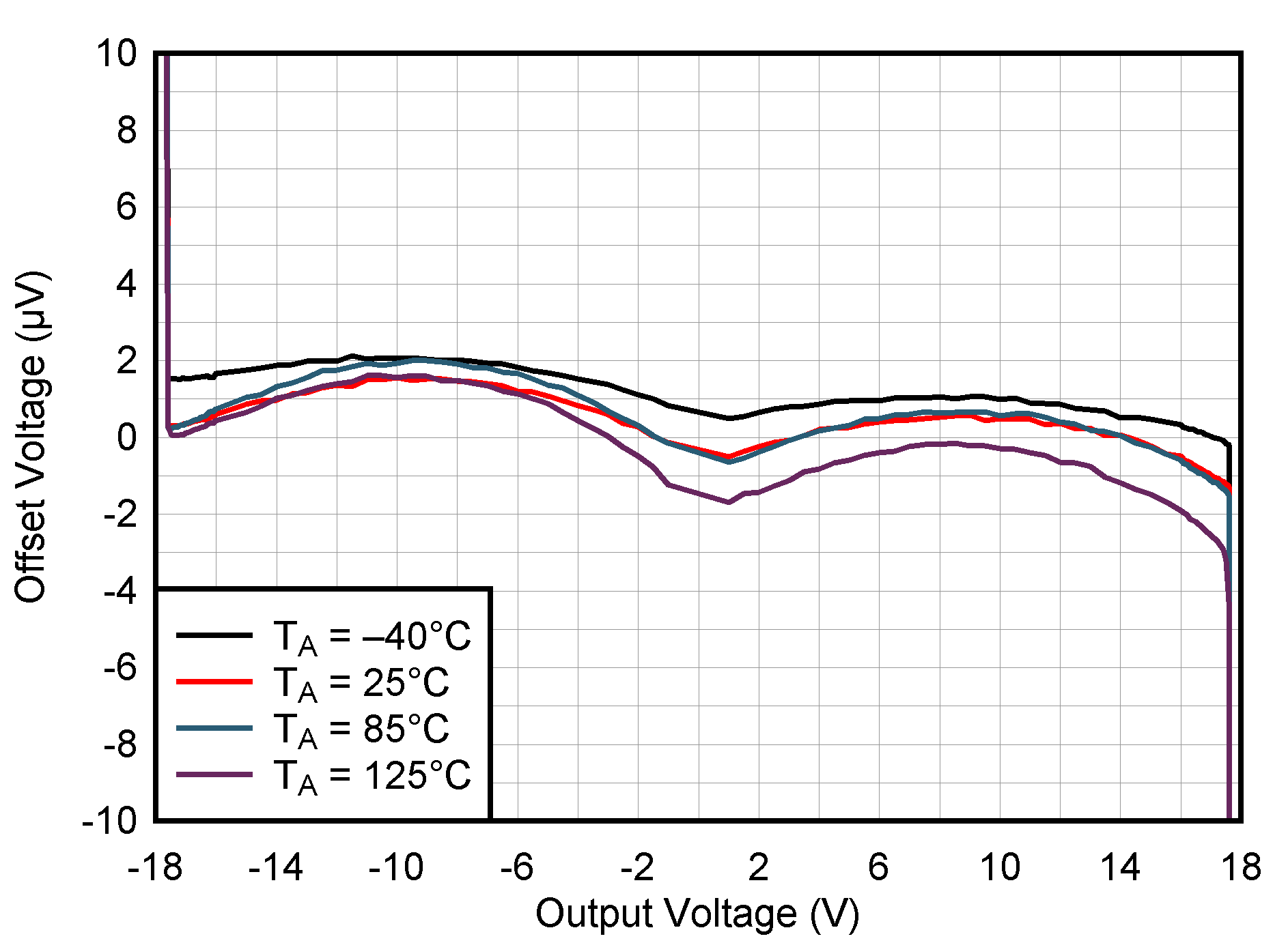
| Offset Voltage vs Output Voltage | Figure 6-6 |
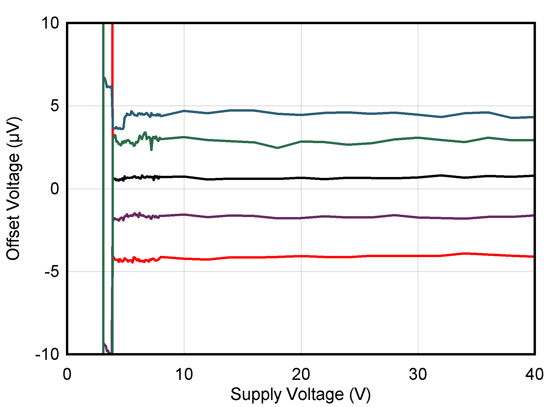
| Offset Voltage vs Power Supply Voltage | Figure 6-7 |
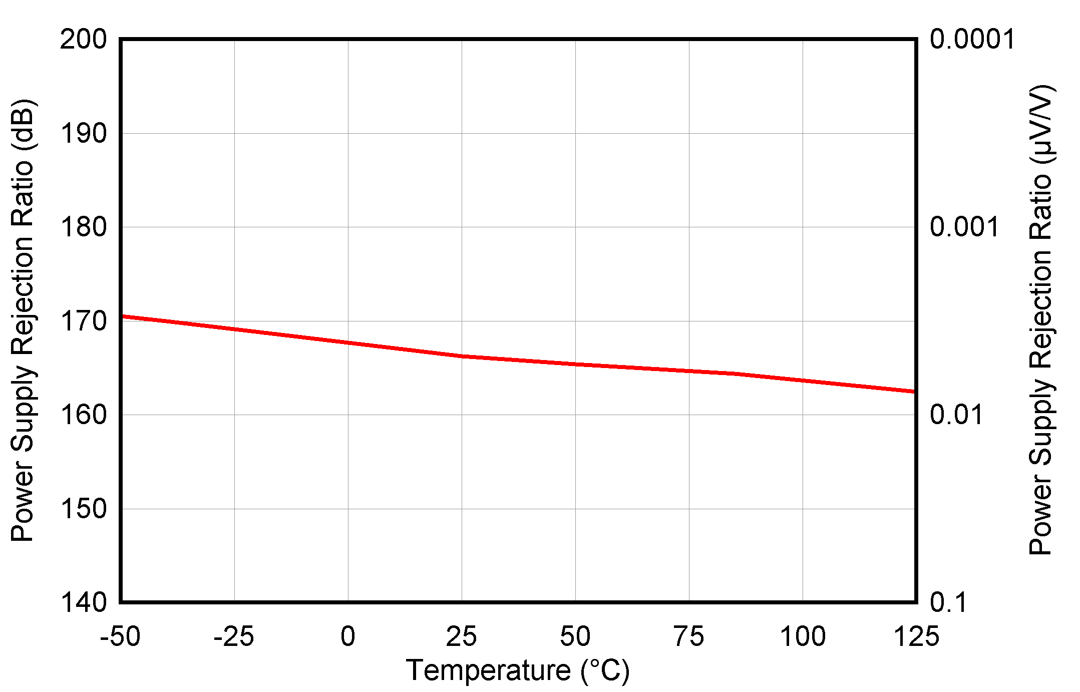
| Power-Supply Rejection Ratio vs Temperature | Figure 6-8 |
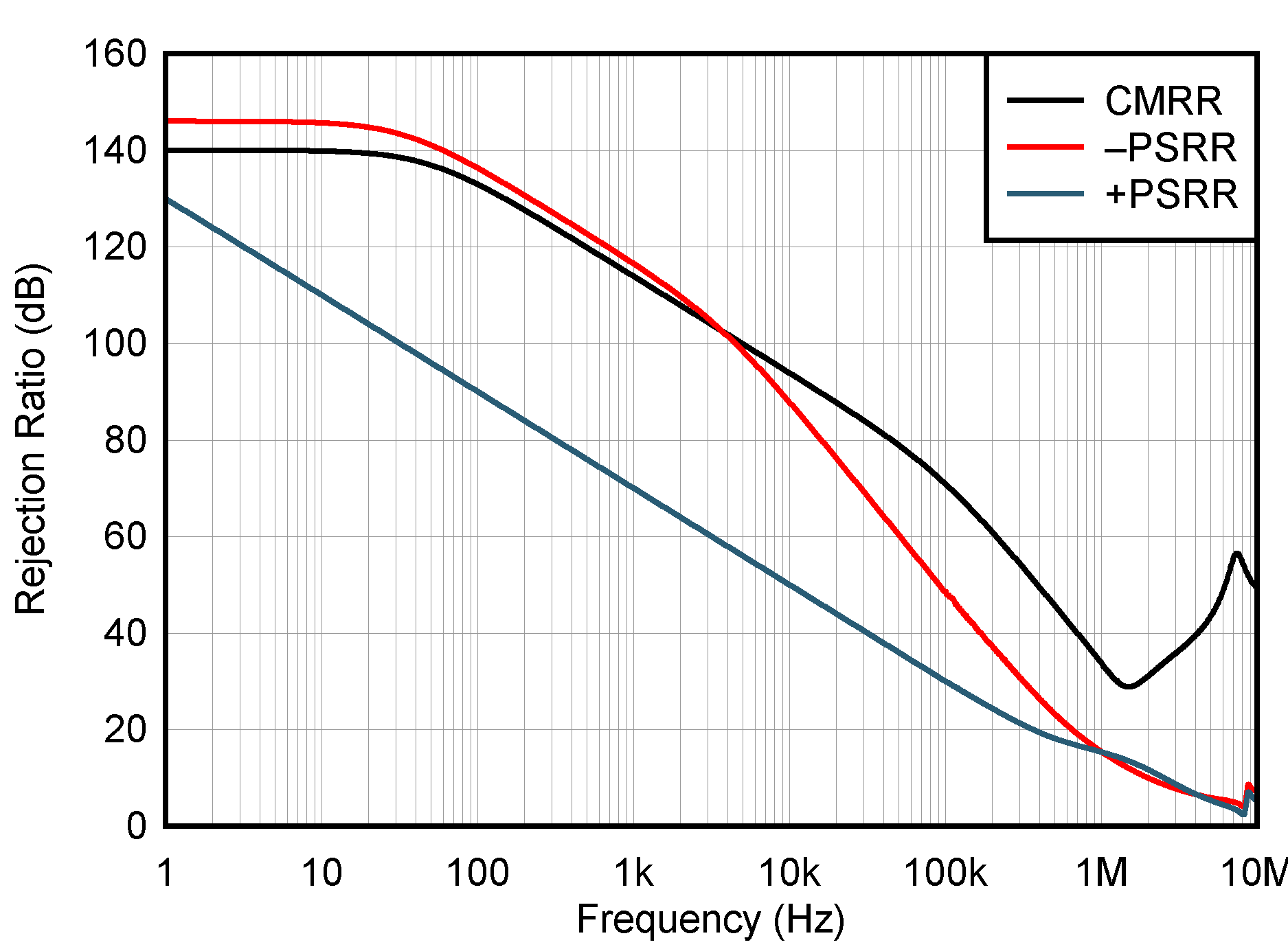
| Power-Supply and Common-Mode Rejection Ratio vs Frequency | Figure 6-9 |
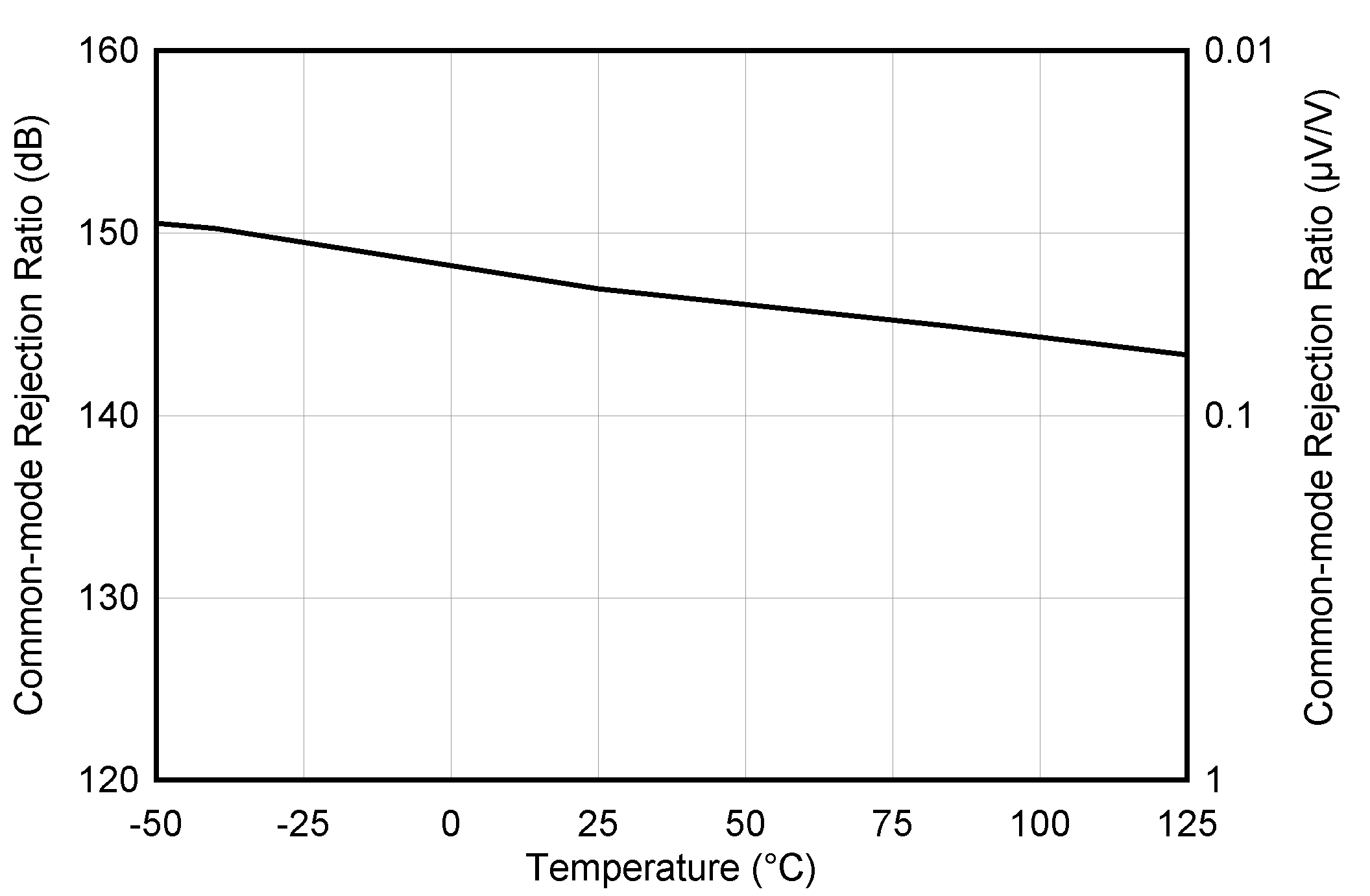
| Common-Mode Rejection Ratio vs Temperature | Figure 6-10 |
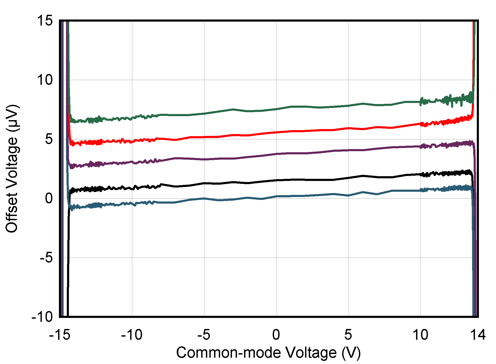
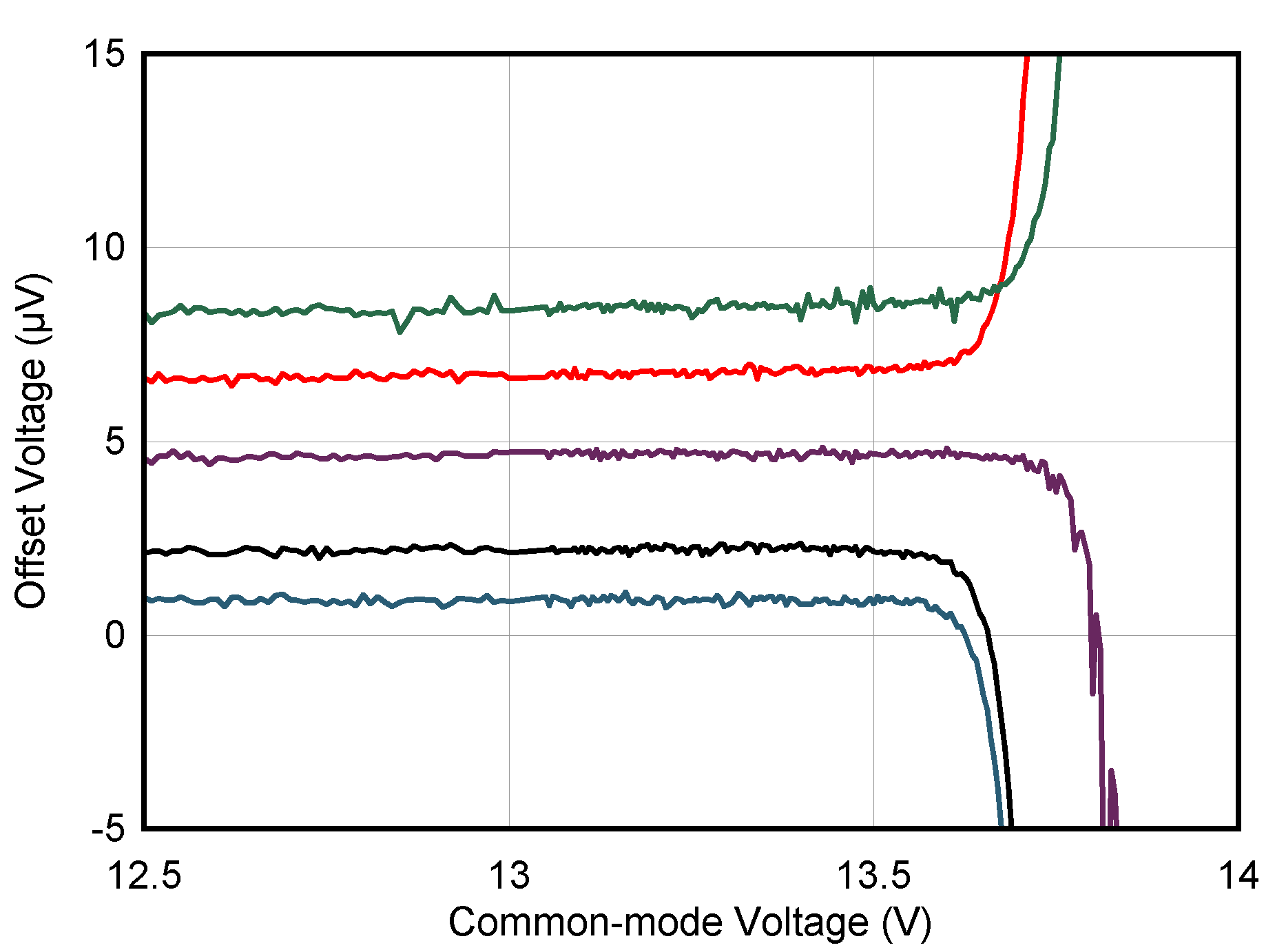
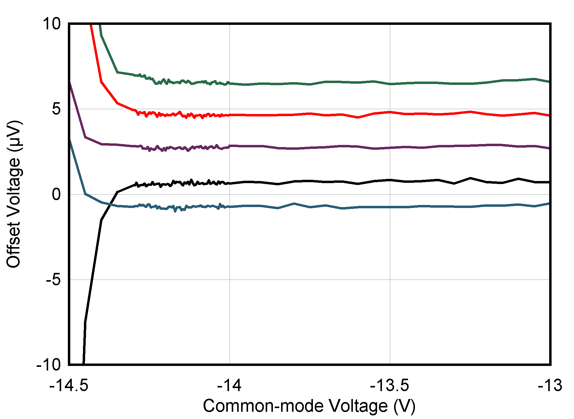
| Offset Voltage vs Common-Mode Voltage | Figure 6-11 |
| Offset Voltage vs VCM at Low Supply | Figure 6-12 |
| Offset Voltage vs VCM at High Supply | Figure 6-13 |
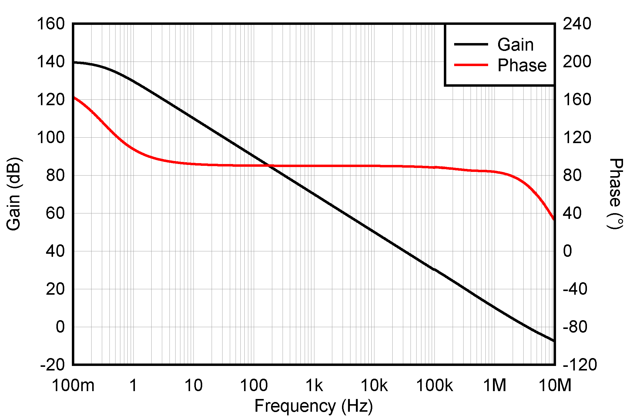
| Open-Loop Gain and Phase vs Frequency | Figure 6-14 |
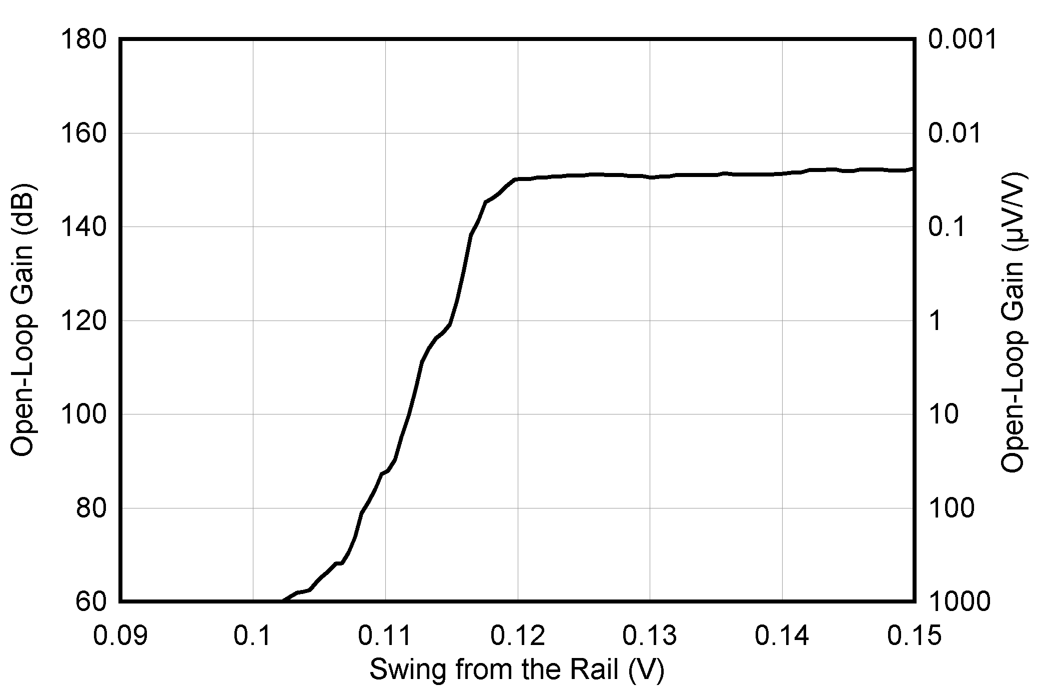
| Open-Loop Gain vs Swing From the Rail | Figure 6-15 |
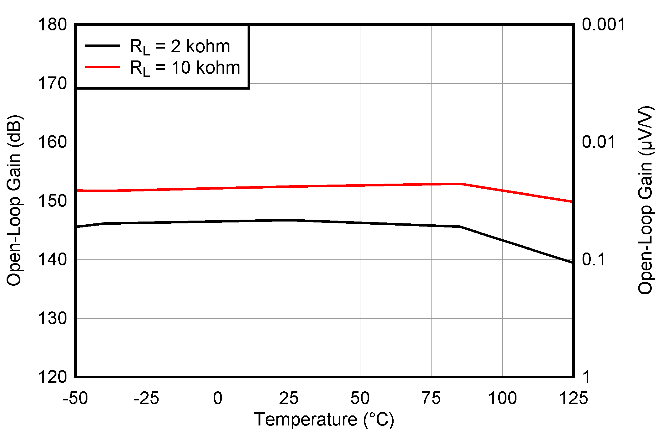
| Open-Loop Gain vs Temperature | Figure 6-16 |
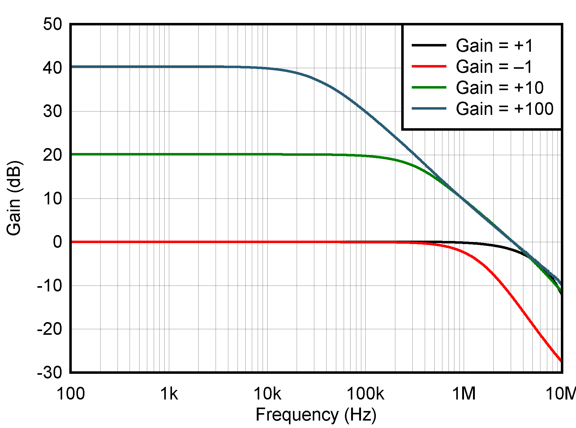
| Closed-Loop Gain vs Frequency | Figure 6-17 |
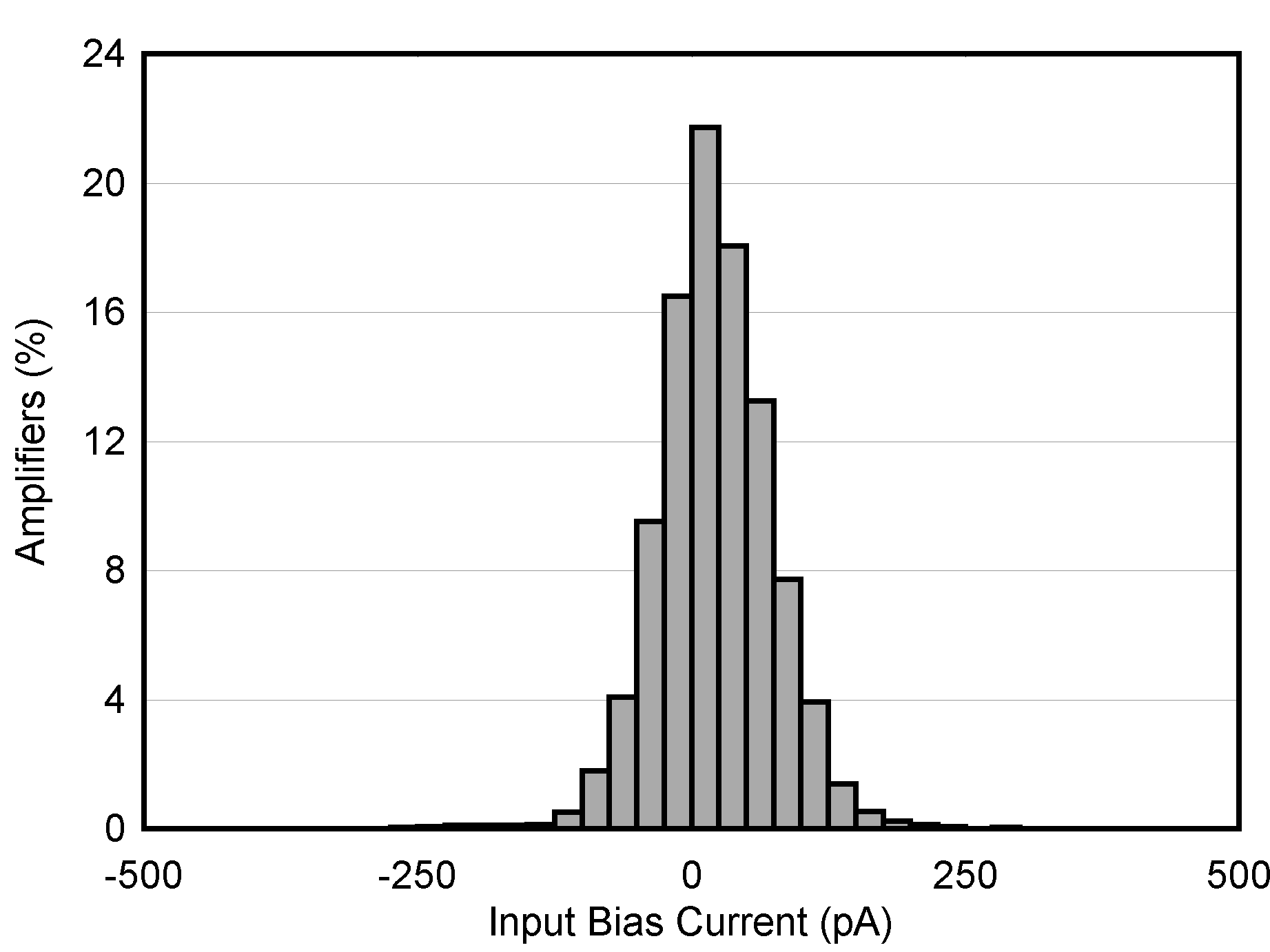
| Input Bias Production Distribution | Figure 6-18 |
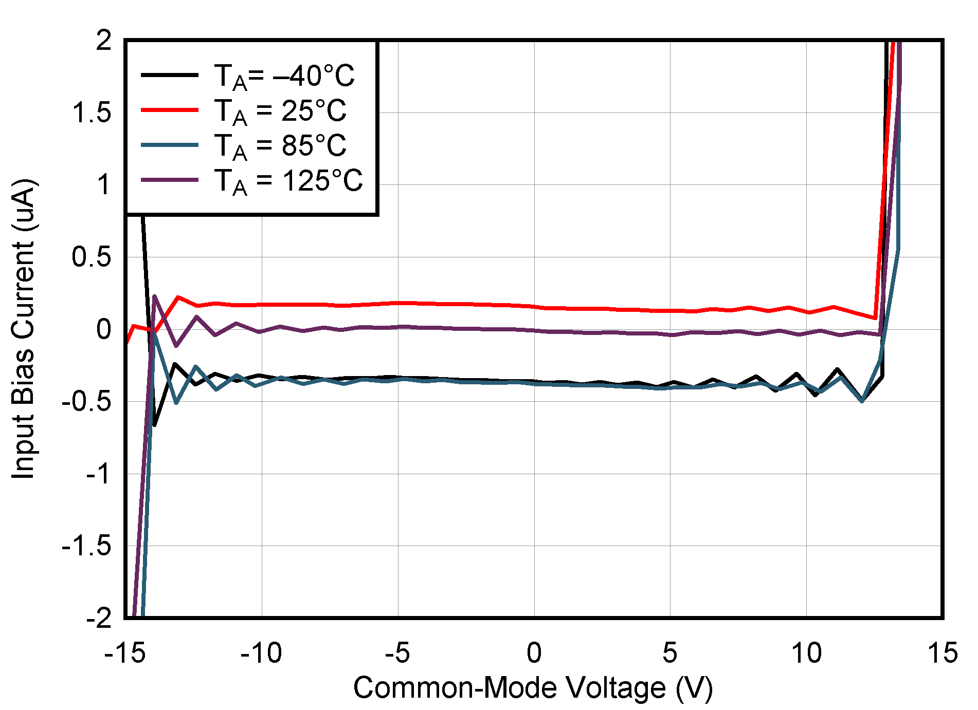
| Input Bias vs Common-Mode Voltage | Figure 6-19 |
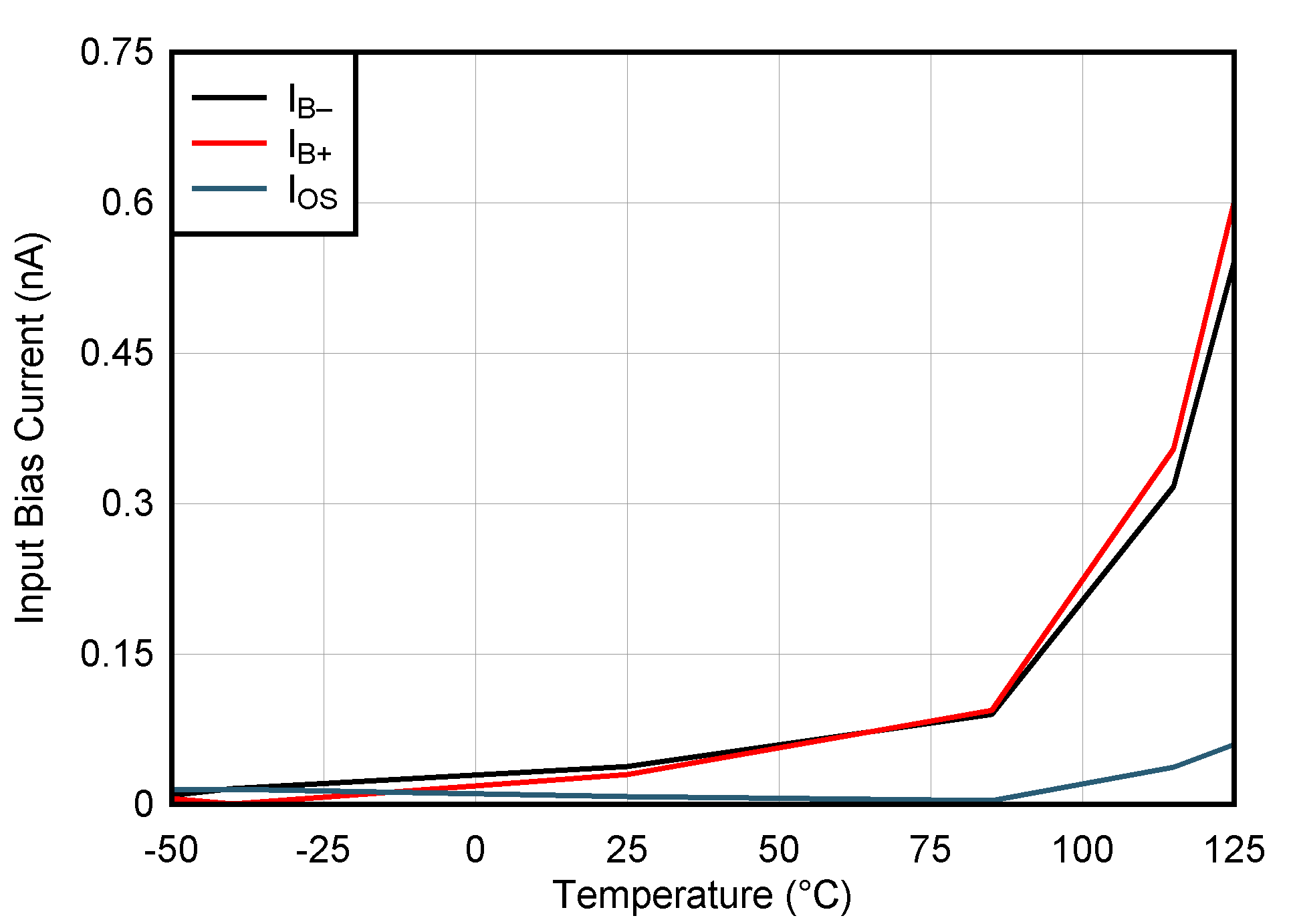
| Input Bias and Input Offset Current vs Temperature | Figure 6-20 |
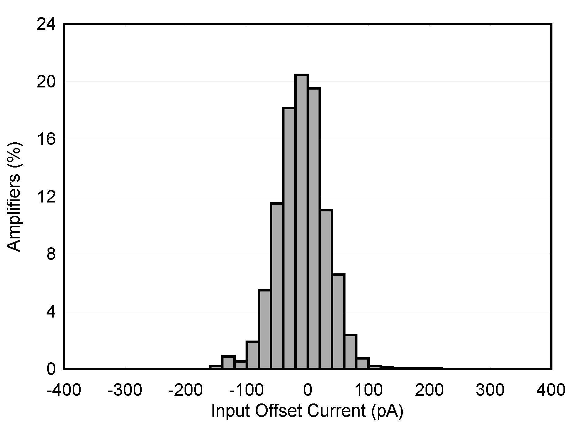
| Input Offset Current Production Distribution | Figure 6-21 |
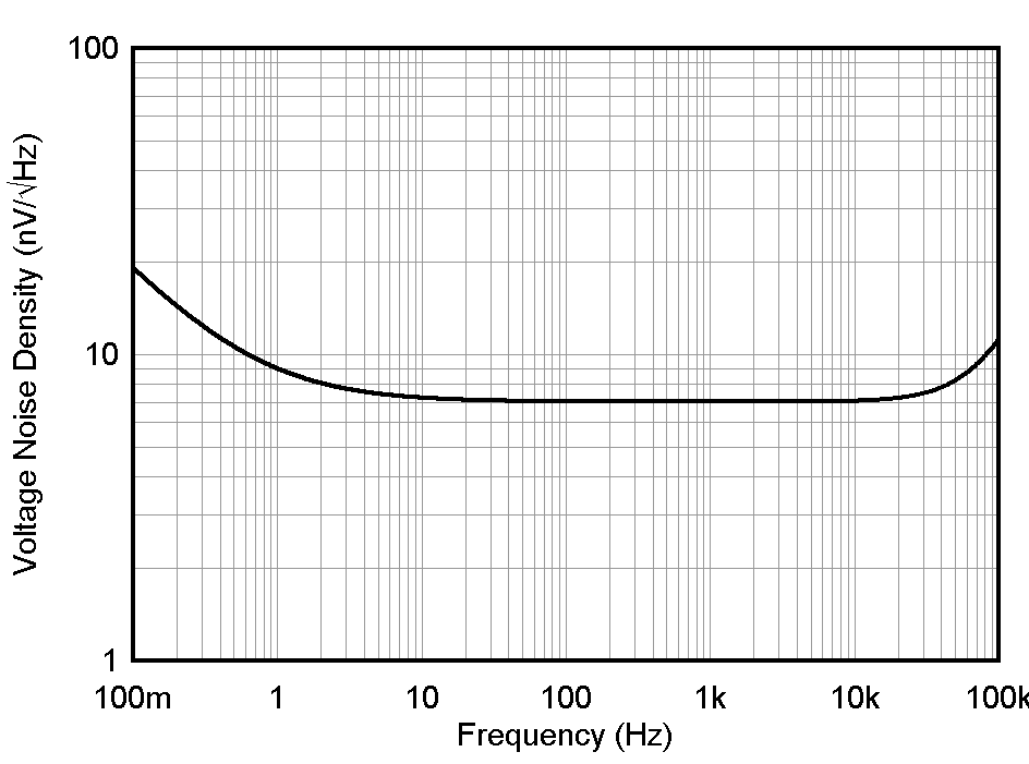
| Voltage Noise Density vs Frequency | Figure 6-22 |
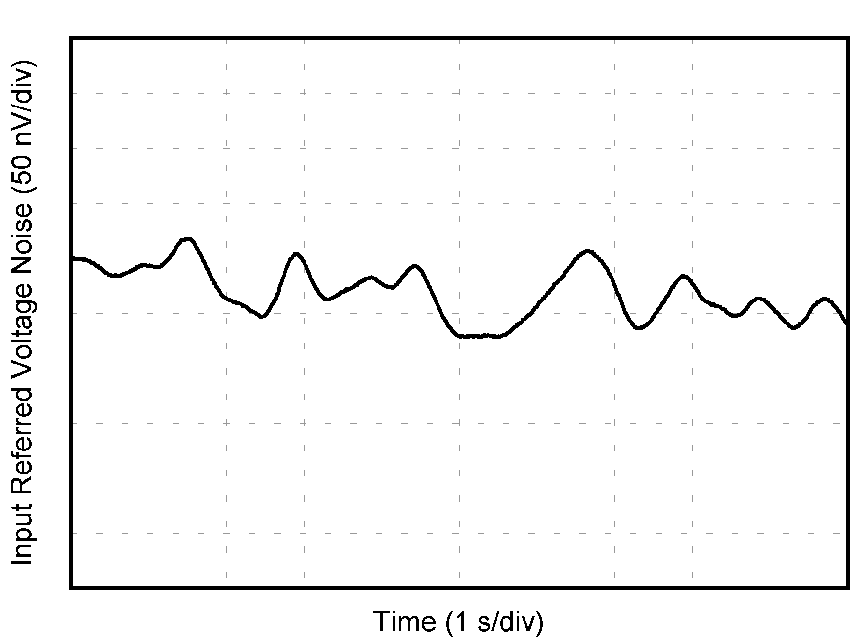
| 0.1-Hz to 10-Hz Noise | Figure 6-23 |
| Total Harmonic Distortion + Noise Ratio vs Frequency | Figure 6-24 |
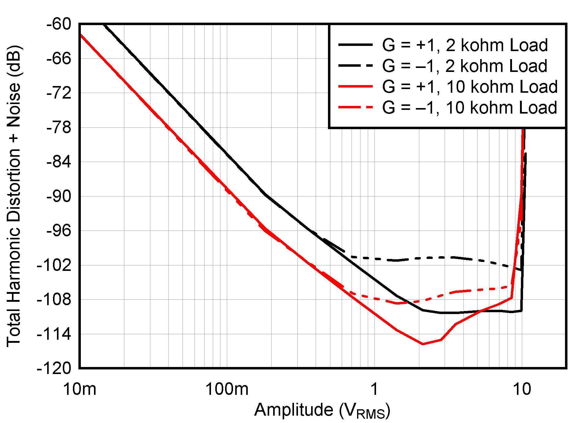
| Total Harmonic Distortion + Noise Ratio vs Output Amplitude | Figure 6-25 |
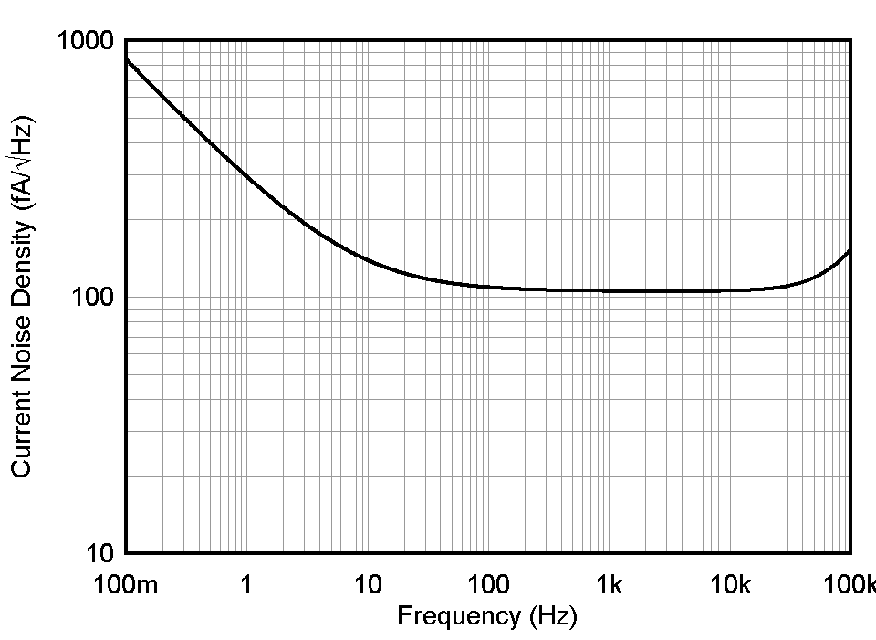
| Current Noise vs Frequency | Figure 6-26 |
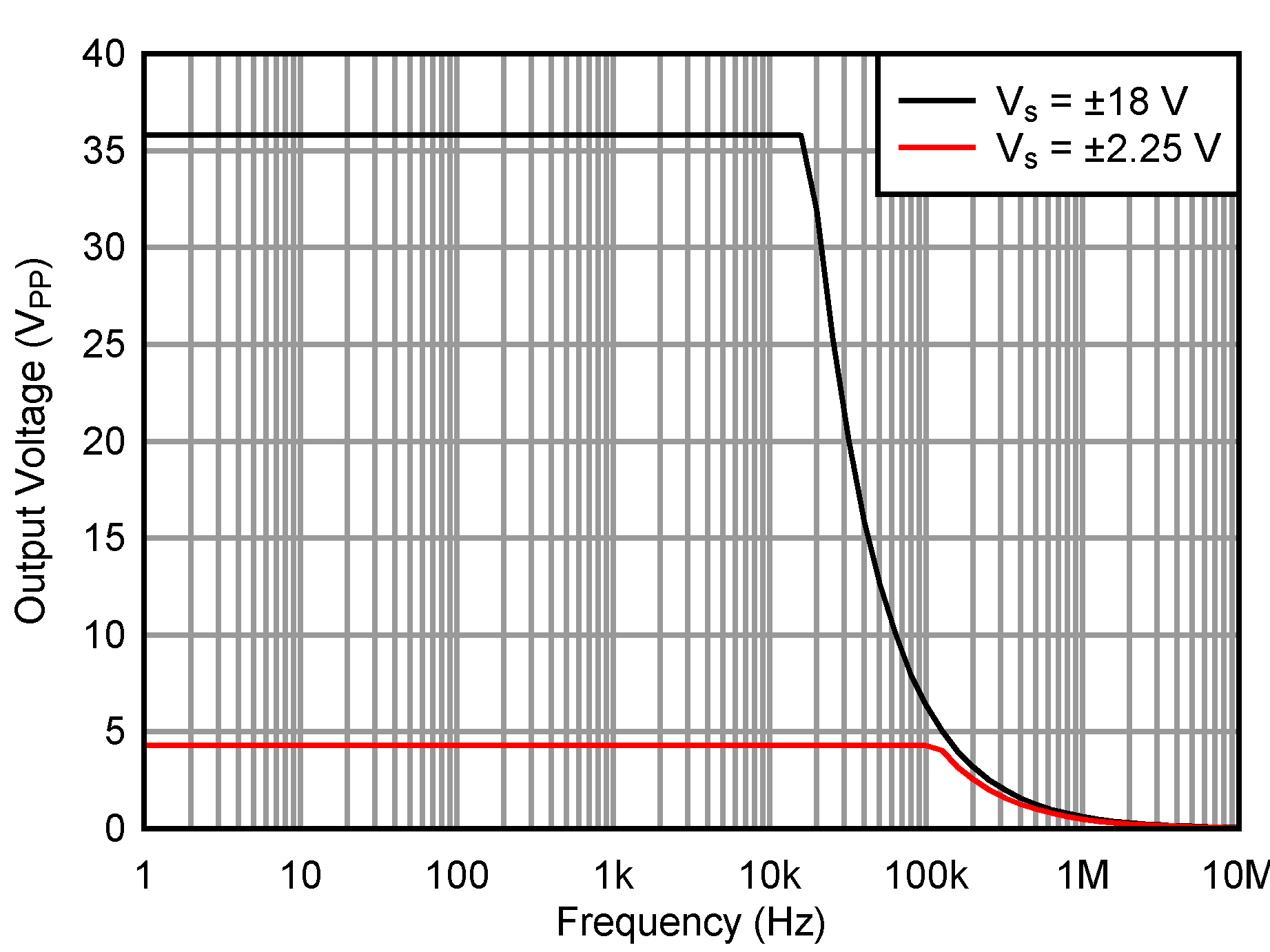
| Maximum Output Voltage vs Frequency | Figure 6-27 |
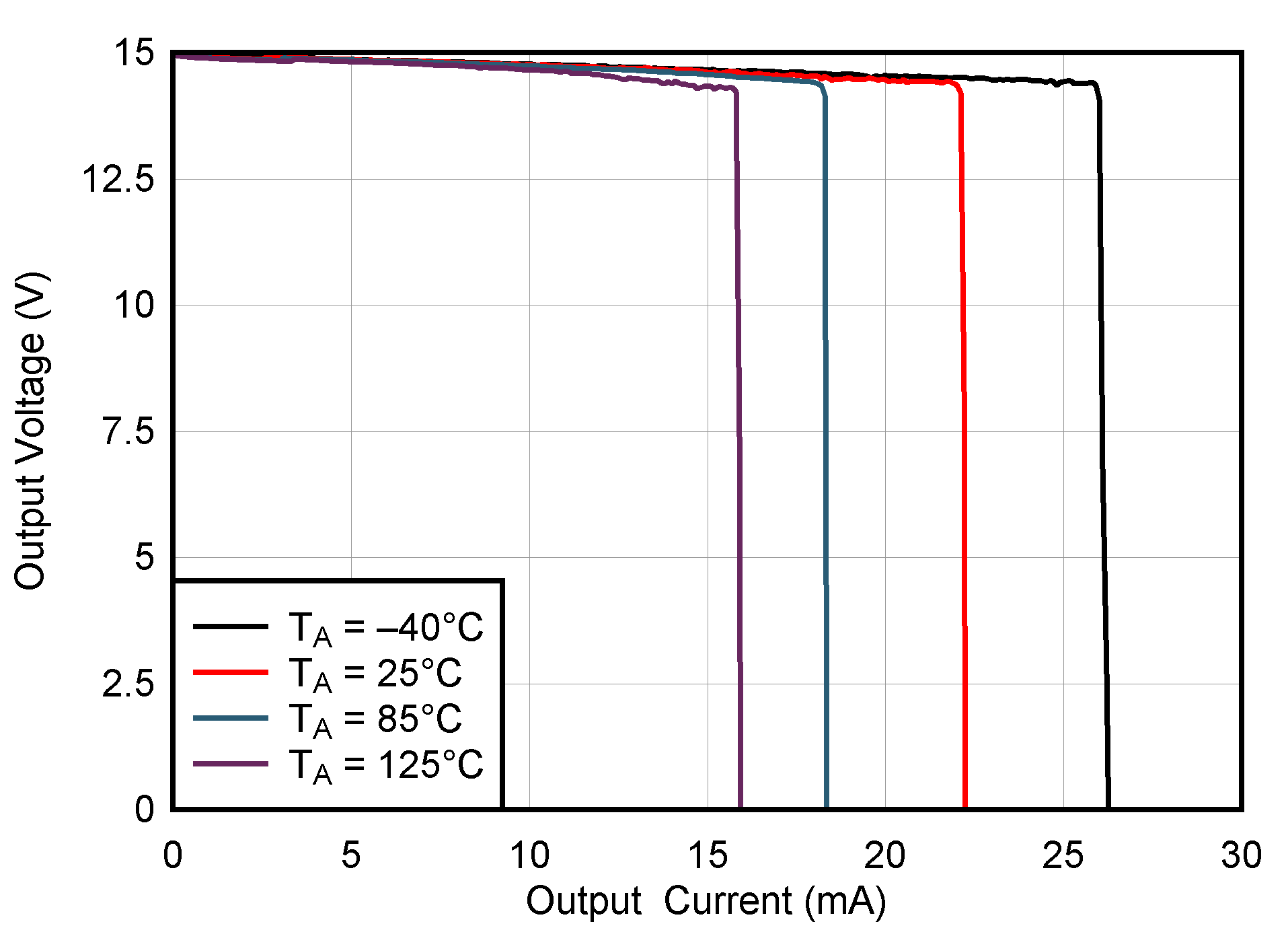
| Output Voltage Swing vs Output Sourcing Current | Figure 6-28 |
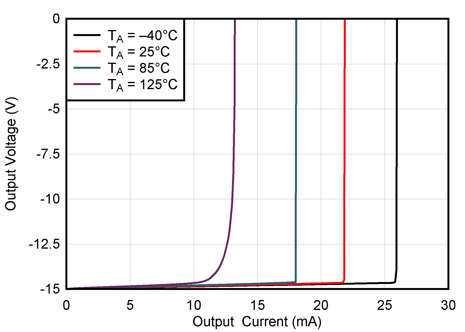
| Output Voltage Swing vs Output Sinking Current | Figure 6-29 |
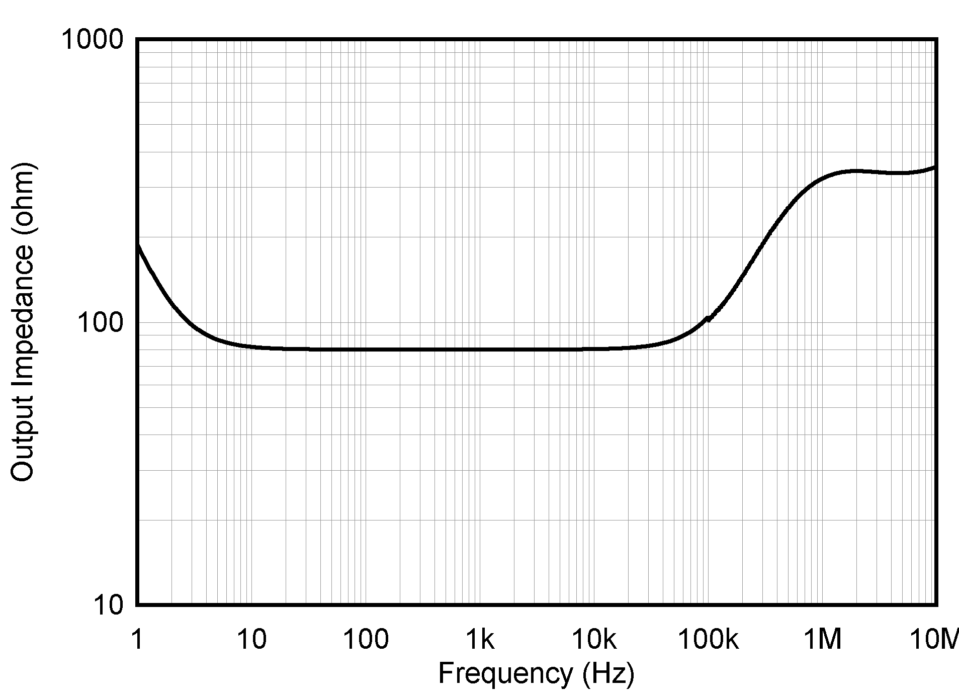
| Open-Loop Output Impedance vs Frequency | Figure 6-30 |
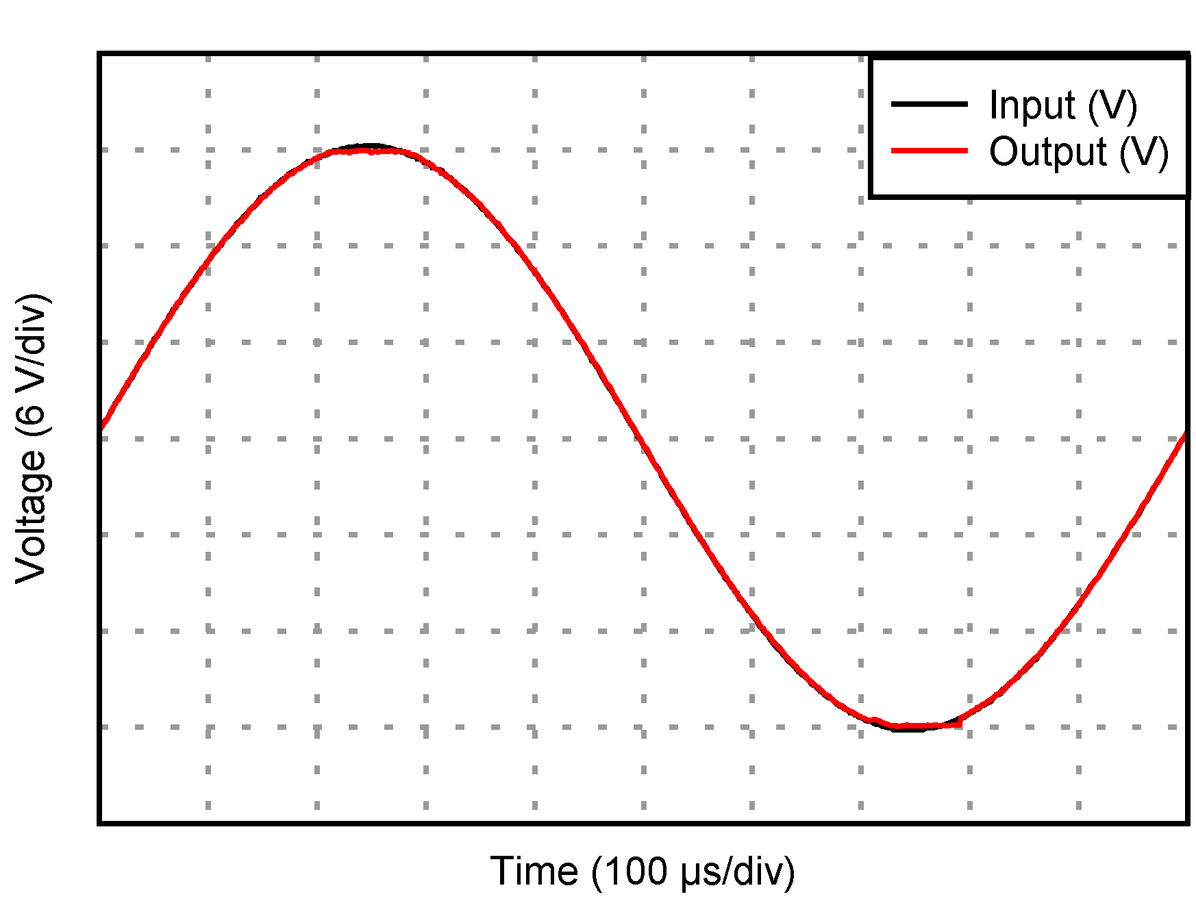
| No Phase Reversal | Figure 6-31 |
| Small-Signal Overshoot vs Capacitive Load, Gain = +1 | Figure 6-32 |
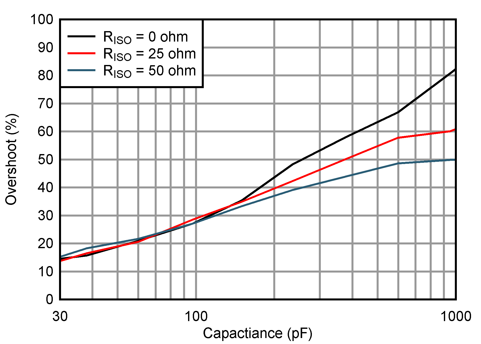
| Small-Signal Overshoot vs Capacitive Load, Gain = –1 | Figure 6-33 |
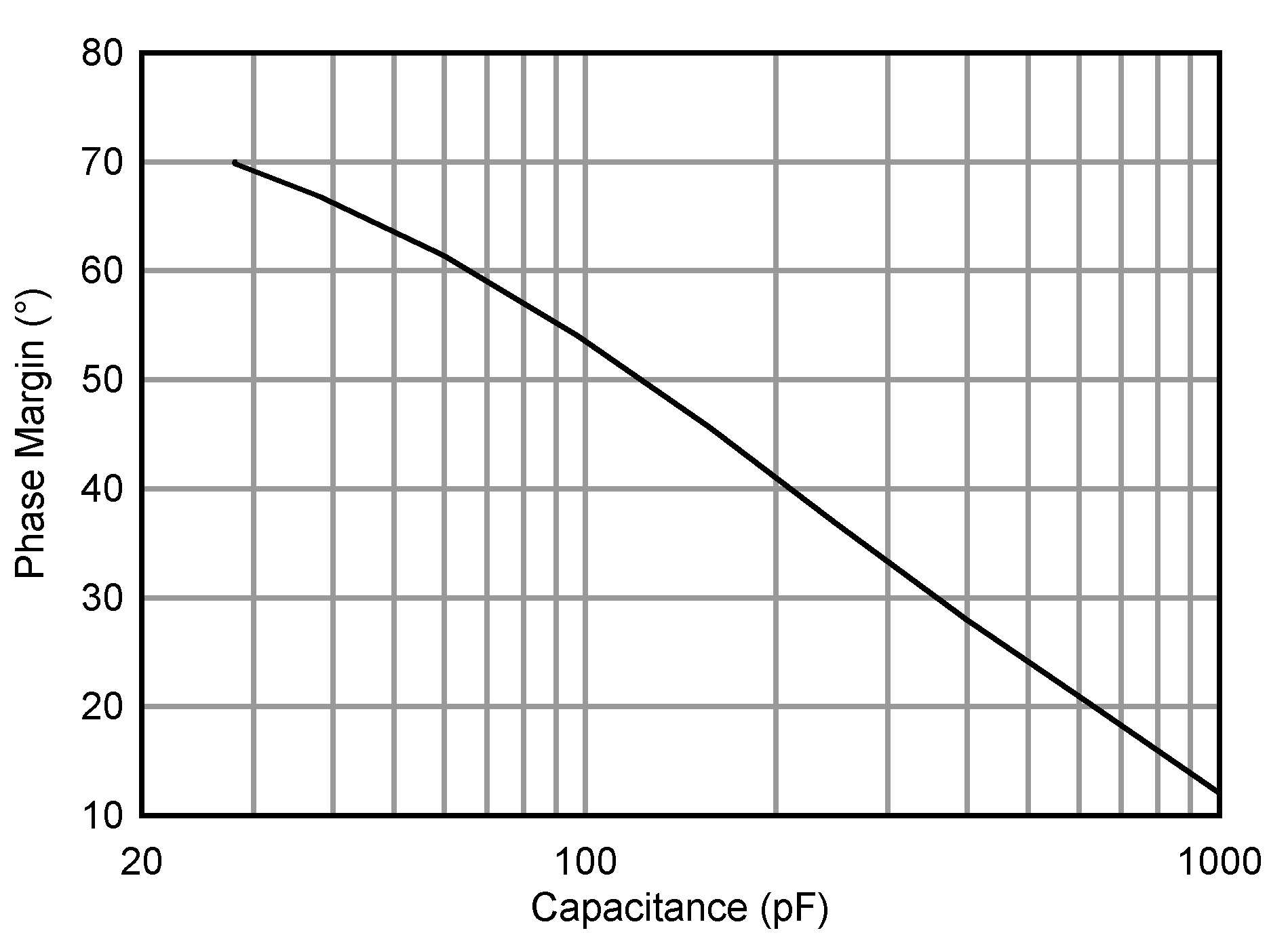
| Phase Margin vs Capacitive Load | Figure 6-34 |
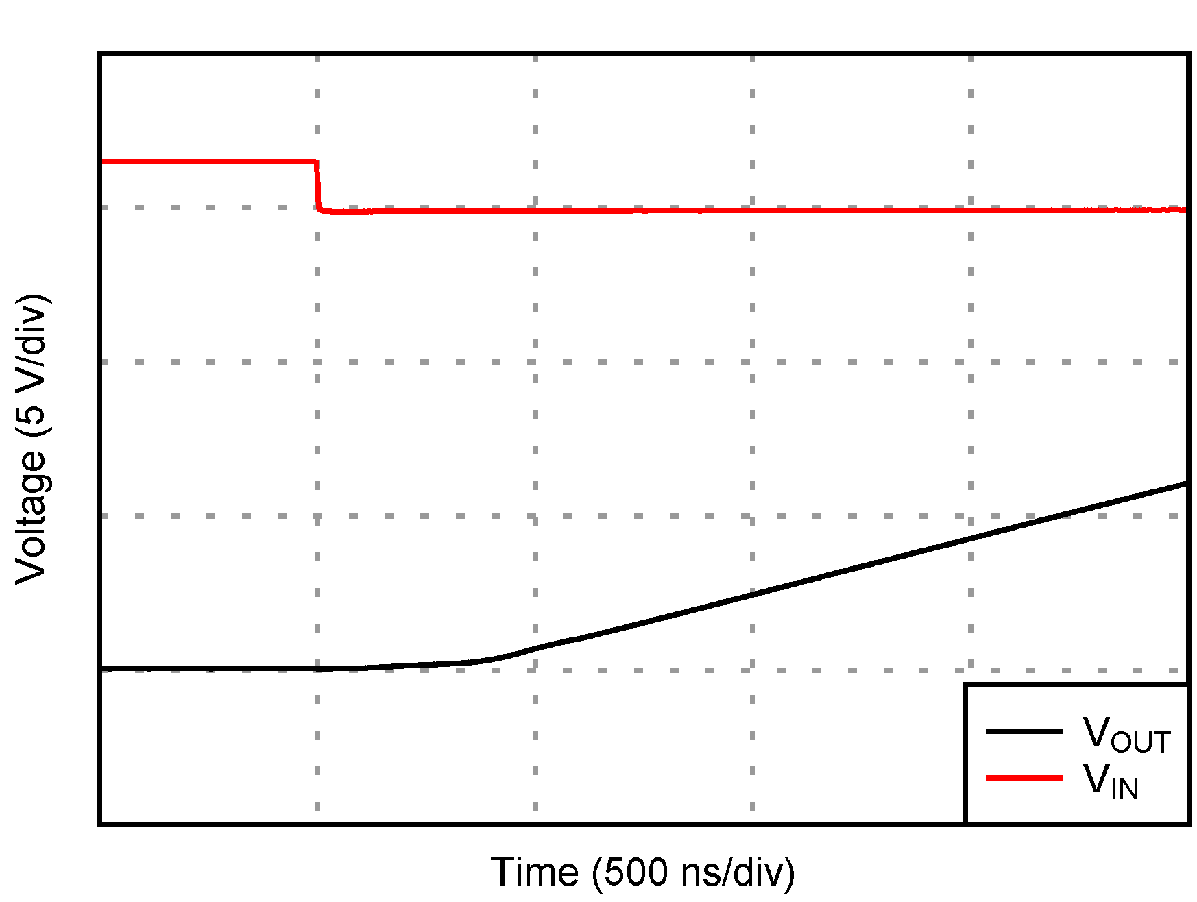
| Positive Overload Recovery, Gain = –1 | Figure 6-35 |
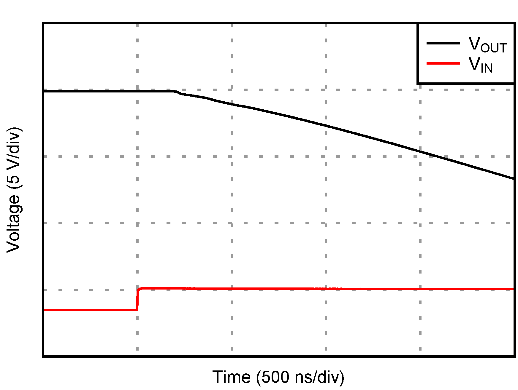
| Negative Overload Recovery, Gain = –1 | Figure 6-36 |
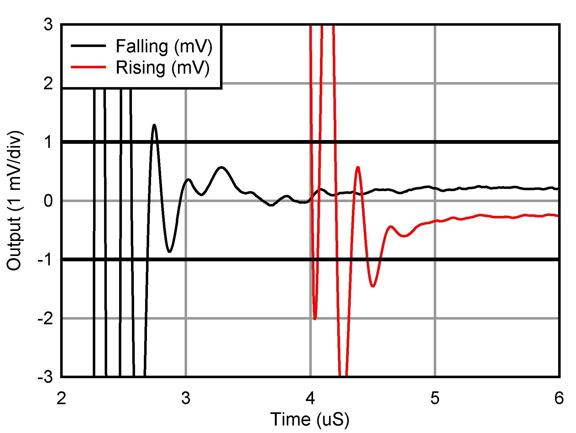
| Settling Time | Figure 6-37 |
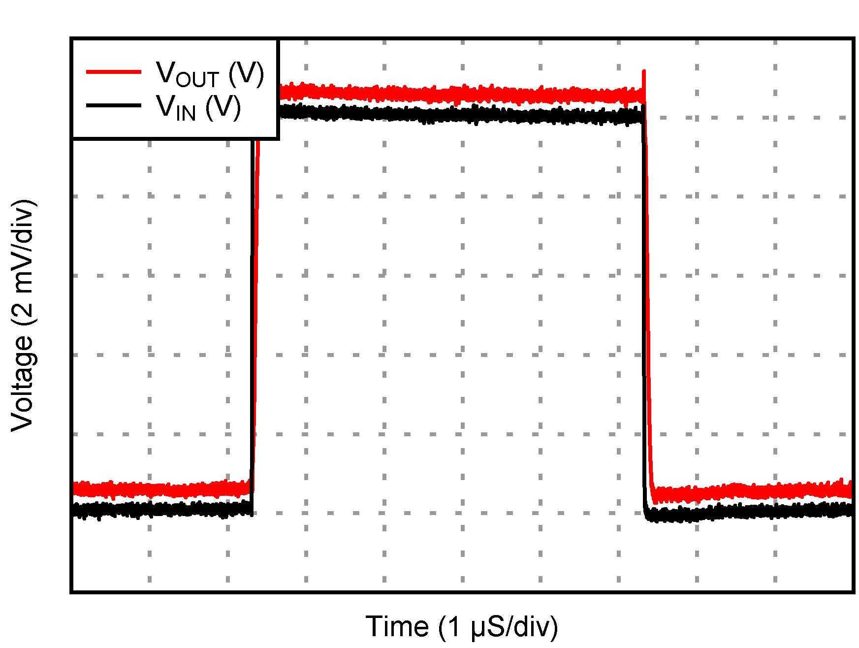
| Small-Signal Step Response, Gain = +1 | Figure 6-38 |
| Small-Signal Step Response, Gain = –1 | Figure 6-39 |
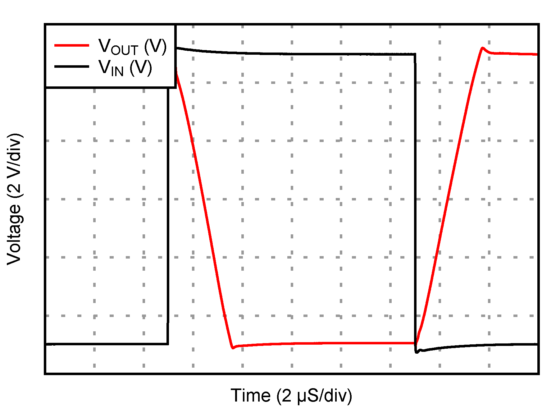
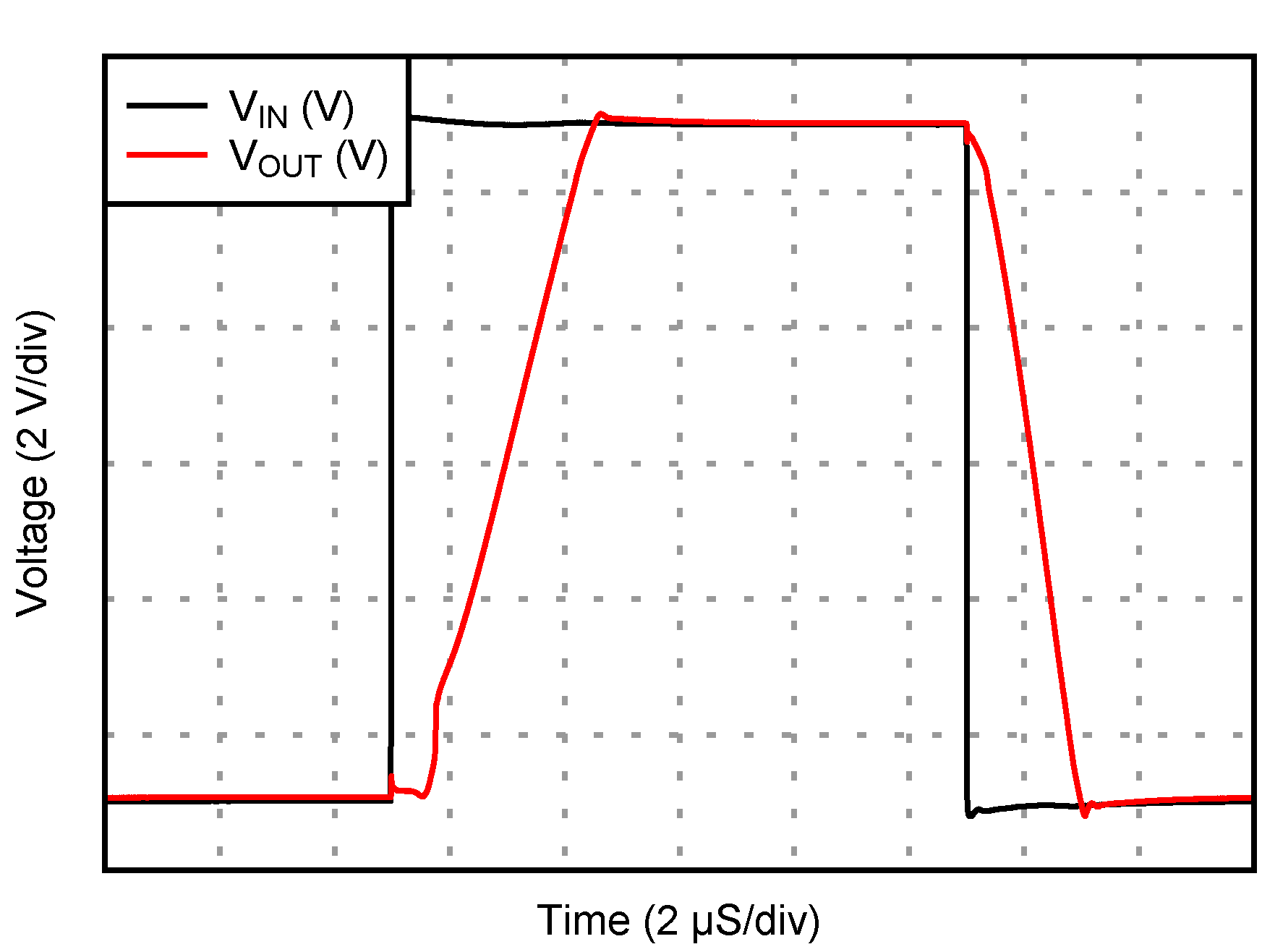
| Large-Signal Step Response, Gain = +1 | Figure 6-40 |
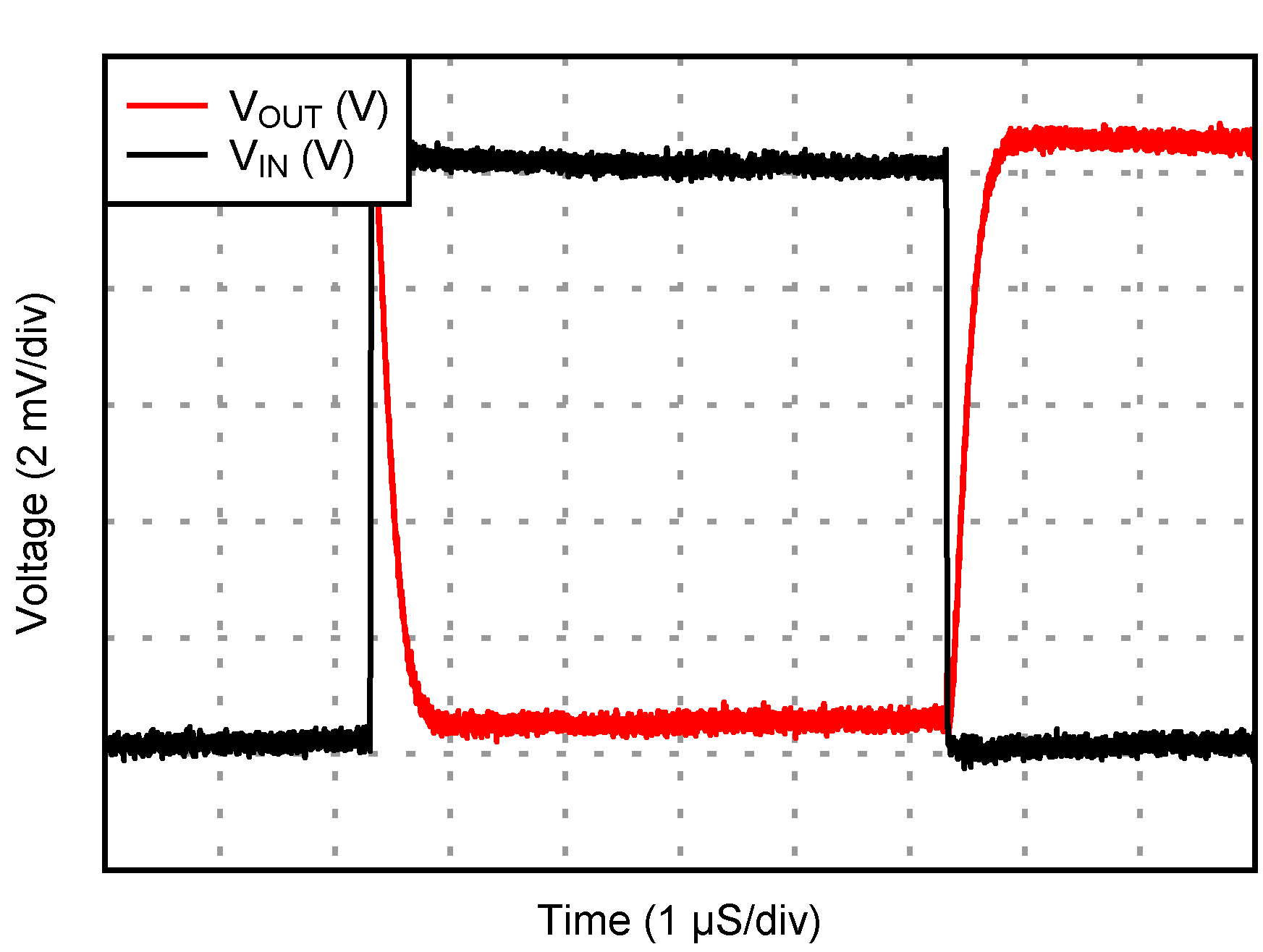
| Large-Signal Step Response, Gain = –1 | Figure 6-41 |
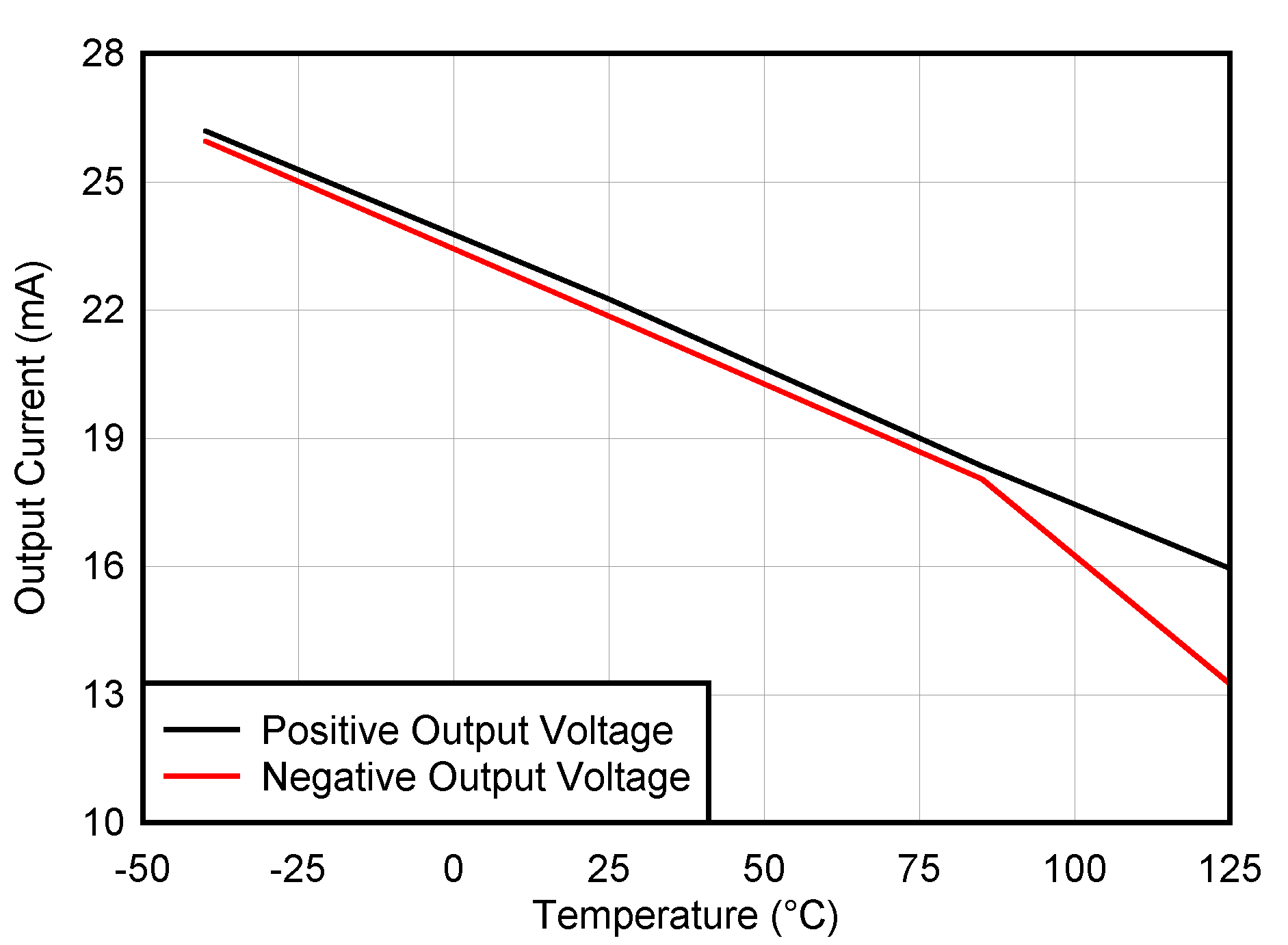
| Short-Circuit Current vs Temperature | Figure 6-42 |
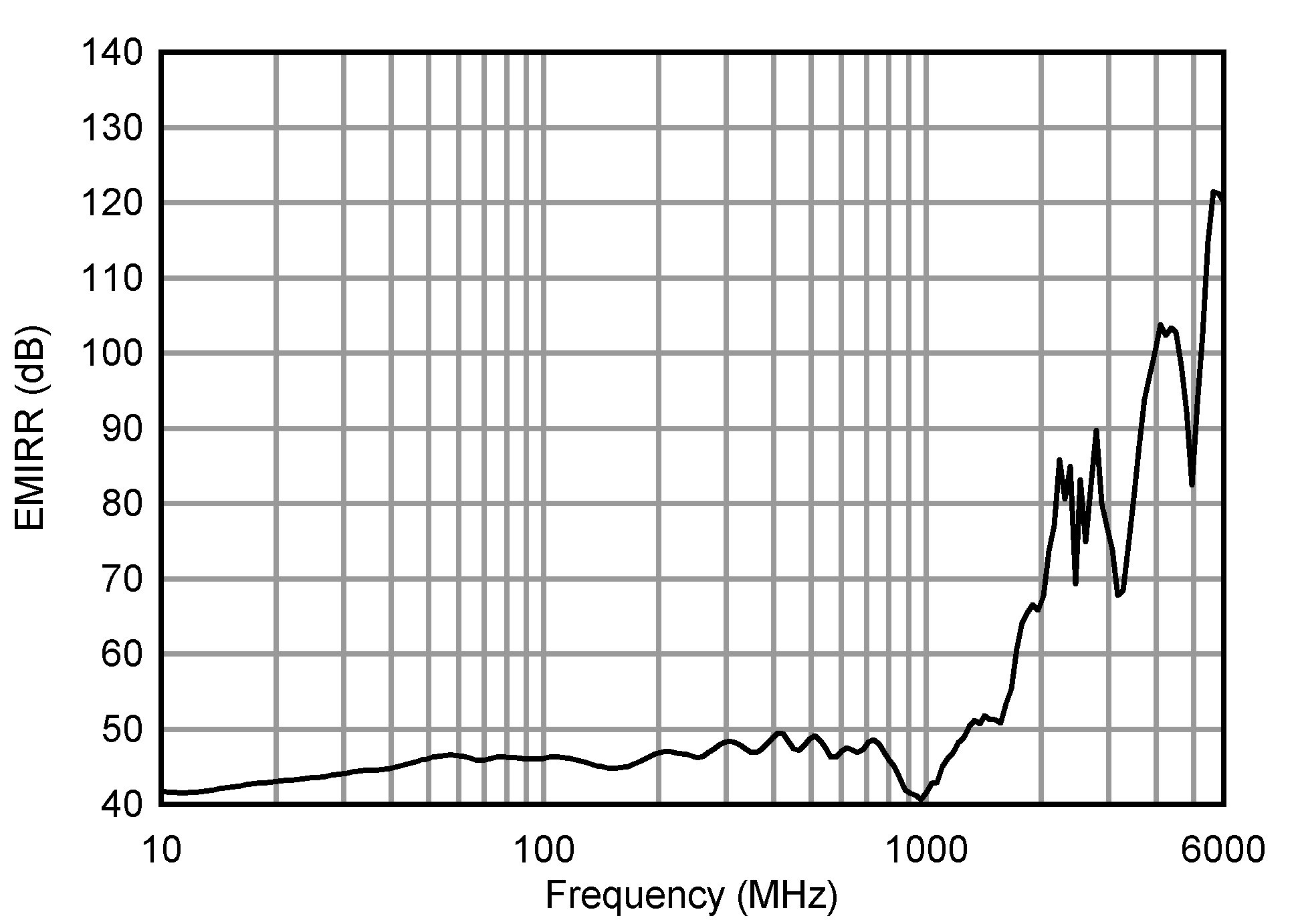
| Electromagnetic Interference Rejection (EMIRR) | Figure 6-43 |
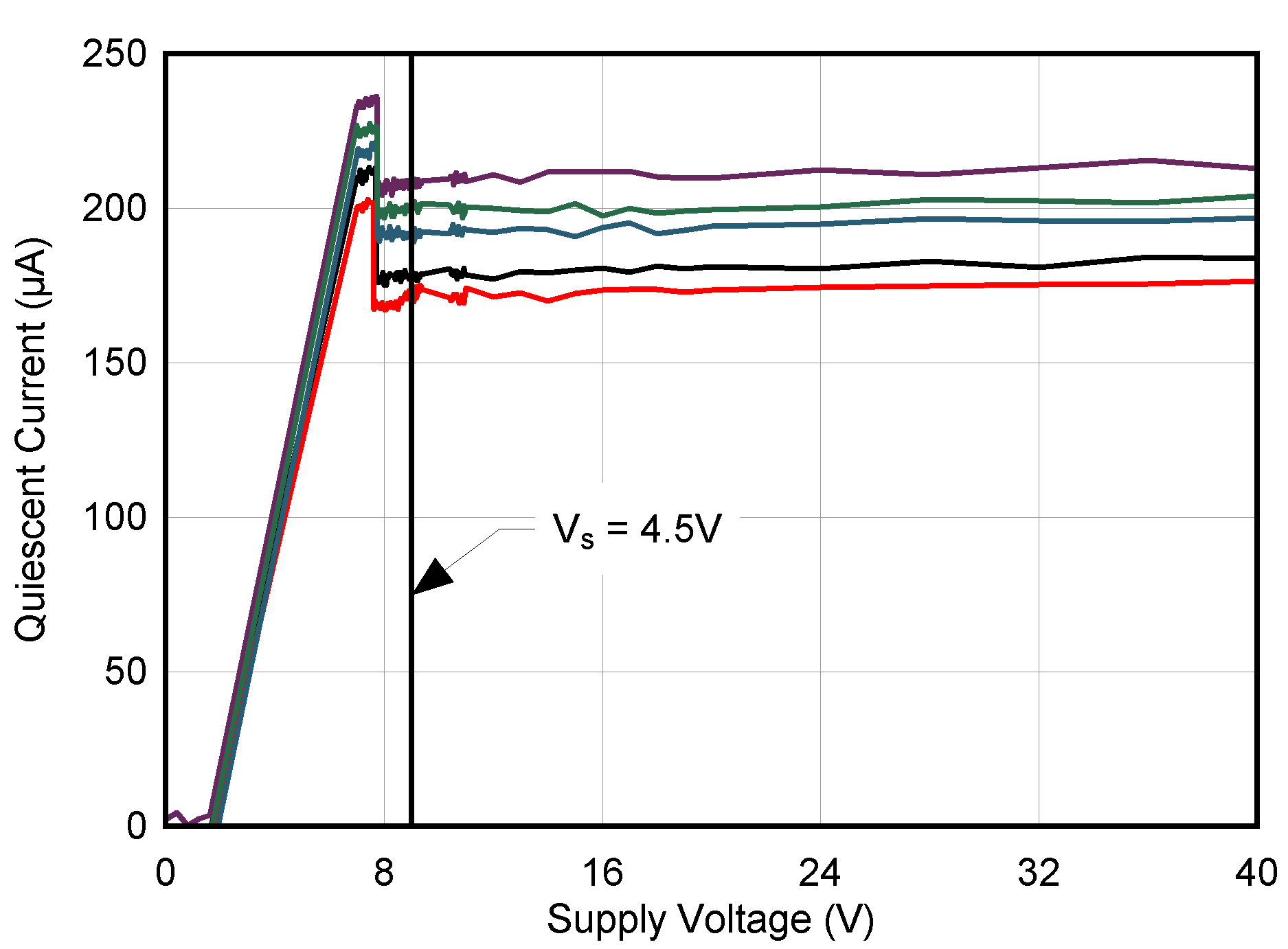
| Quiescent Current vs Supply Voltage | Figure 6-44 |
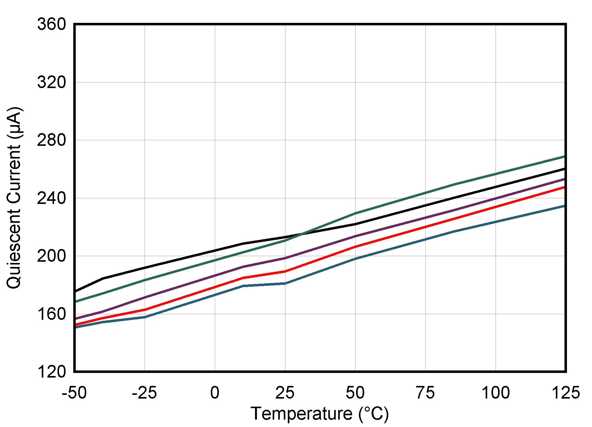
| Quiescent Current vs Temperature | Figure 6-45 |
| TA = 25°C |
| TA = –40°C |
vs Output Amplitude
| Gain = –1 |
Gain = –1
| Gain = –1 |
| Gain = –1 |
| Gain = –1 |
| TA = 125°C |
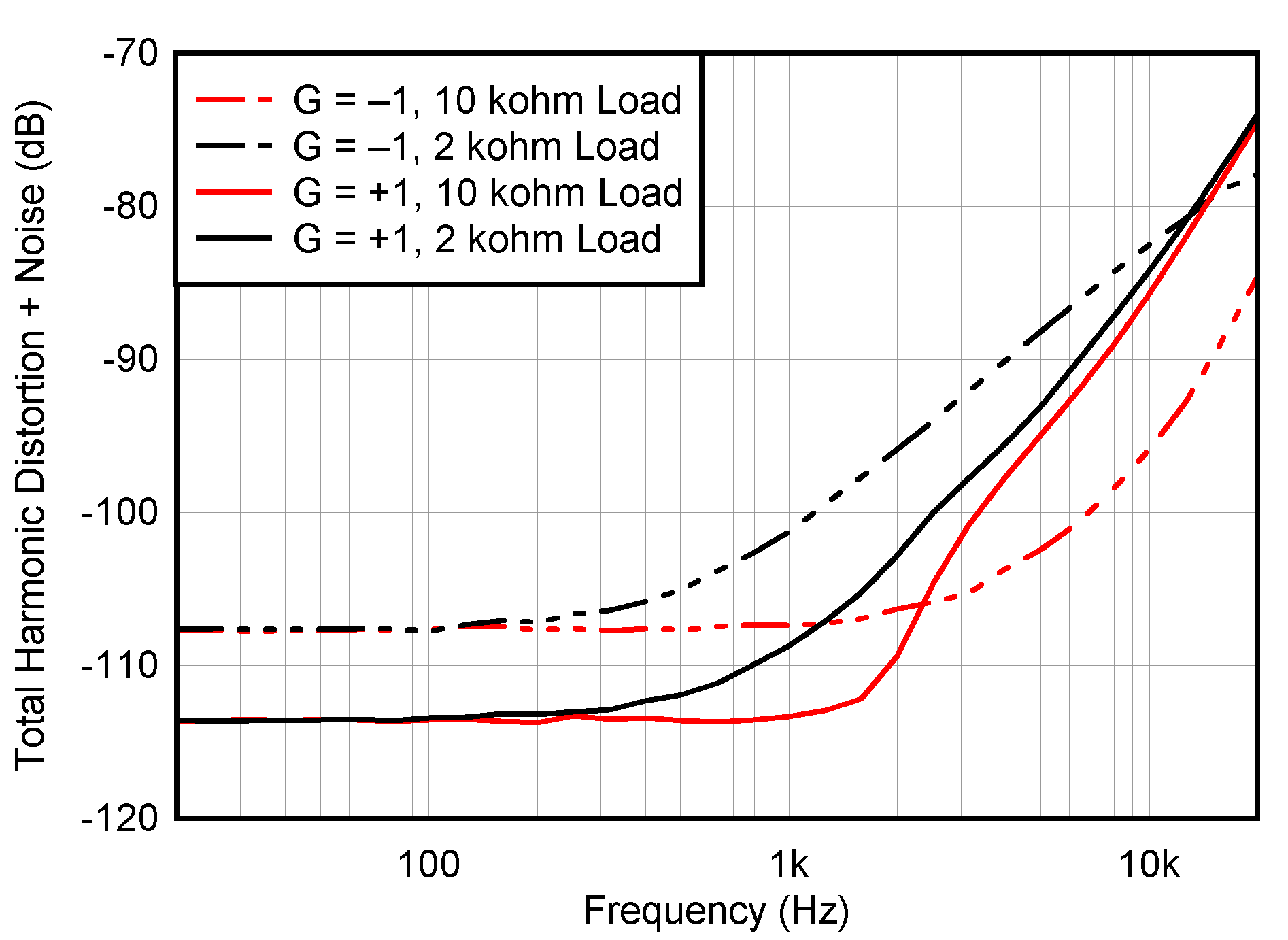
vs Frequency
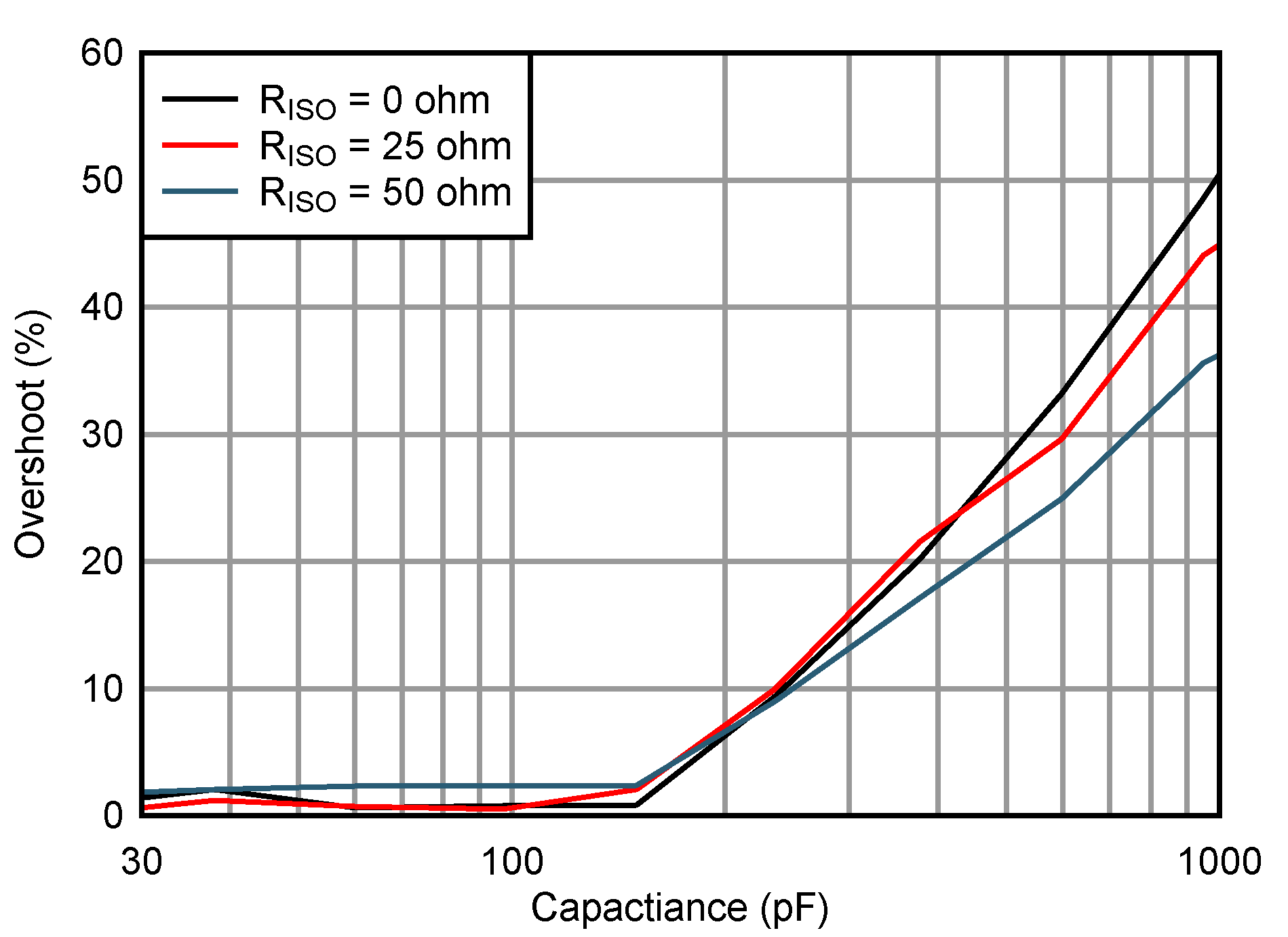
| Gain = 1 |
Gain = +1
| Gain = –1 |
| Gain = 1 |
| Gain = 1 |
