ZHCSIR5H September 2018 – August 2021 OPA210 , OPA2210
PRODUCTION DATA
- 1 特性
- 2 应用
- 3 说明
- 4 Revision History
- 5 Pin Configuration and Functions
- 6 Specifications
- 7 Detailed Description
- 8 Application and Implementation
- 9 Power Supply Recommendations
- 10Layout
- 11Device and Documentation Support
- 12Mechanical, Packaging, and Orderable Information
封装选项
机械数据 (封装 | 引脚)
散热焊盘机械数据 (封装 | 引脚)
- DRG|8
订购信息
7.3.2 Input Protection
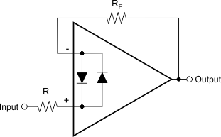
The input pins of the OPAx210 are protected from excessive differential voltage with back-to-back diodes, as shown in Figure 7-1. In most circuit applications, the input protection circuitry has no consequence. However, in low-gain or G = 1 circuits, fast-ramping input signals can forward-bias these diodes because the output of the amplifier cannot respond rapidly enough to the input ramp. This effect is illustrated in Figure 6-35 and Figure 6-36 in Section 6.7. If the input signal is fast enough to create this forward-bias condition, the input signal current must be limited to 10 mA or less. If the input signal current is not inherently limited, an input series resistor can be used to limit the signal input current. This input series resistor degrades the low-noise performance of the OPAx210. See Section 7.3.3 for further information on noise performance.
Figure 7-1 shows an example configuration that implements a current-limiting feedback resistor.
 Figure 7-1 Pulsed Operation