ZHCSED2 November   2015 OPA2211-EP

PRODUCTION DATA.  

  1. 特性
  2. 应用范围
  3. 说明
  4. 修订历史记录
  5. Pin Configuration and Functions
  6. Specifications
    1. 6.1 Absolute Maximum Ratings
    2. 6.2 ESD Ratings
    3. 6.3 Recommended Operating Conditions
    4. 6.4 Thermal Information
    5. 6.5 Electrical Characteristics: VS = ±2.25 to ±18 V
    6. 6.6 Typical Characteristics
  7. Detailed Description
    1. 7.1 Overview
    2. 7.2 Functional Block Diagram
    3. 7.3 Feature Description
      1. 7.3.1 Input Protection
      2. 7.3.2 Noise Performance
      3. 7.3.3 Basic Noise Calculations
      4. 7.3.4 Total Harmonic Distortion Measurements
    4. 7.4 Device Functional Modes
  8. Application and Implementation
    1. 8.1 Application Information
      1. 8.1.1 Electrical Overstress
    2. 8.2 Typical Application
      1. 8.2.1 Design Requirements
      2. 8.2.2 Detailed Design Procedure
        1. 8.2.2.1 Total Harmonic Distortion Measurements
      3. 8.2.3 Application Curves
  9. Power Supply Recommendations
    1. 9.1 Operating Voltage
  10. 10Layout
    1. 10.1 Layout Guidelines
    2. 10.2 Layout Example
    3. 10.3 Thermal Considerations
  11. 11器件和文档支持
    1. 11.1 社区资源
    2. 11.2 商标
    3. 11.3 静电放电警告
    4. 11.4 Glossary
  12. 12机械、封装和可订购信息

封装选项

机械数据 (封装 | 引脚)
散热焊盘机械数据 (封装 | 引脚)
订购信息

5 Pin Configuration and Functions

DRG Package
8-Pin WSON
Top View
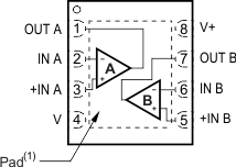
OPA2211-EP po_DRG_bos638.gif
1. Exposed thermal die pad on underside; connect thermal die pad to V–. Soldering the thermal pad improves heat dissipation and provides specified performance

Pin Functions

PIN I/O DESCRIPTION
NAME NO.
+IN A 3 I Noninverting input for channel A
–IN A 2 I Inverting input for channel A
+IN B 5 I Noninverting input for channel B
–IN B 6 I Inverting input for channel B
OUT A 1 O Output terminal for channel A
OUT B 7 O Output terminal for channel B
V+ 8 Positive supply voltage
V– 4 Negative supply voltage