ZHCSED2 November 2015 OPA2211-EP
PRODUCTION DATA.
8 Application and Implementation
NOTE
Information in the following applications sections is not part of the TI component specification, and TI does not warrant its accuracy or completeness. TI’s customers are responsible for determining suitability of components for their purposes. Customers should validate and test their design implementation to confirm system functionality.
8.1 Application Information
8.1.1 Electrical Overstress
Designers often ask questions about the capability of an operational amplifier to withstand electrical overstress. These questions tend to focus on the device inputs, but may involve the supply voltage pins or even the output pin. Each of these different pin functions have electrical stress limits determined by the voltage breakdown characteristics of the particular semiconductor fabrication process and specific circuits connected to the pin. Additionally, internal electrostatic discharge (ESD) protection is built into these circuits to protect them from accidental ESD events both before and during product assembly.
It is helpful to have a good understanding of this basic ESD circuitry and its relevance to an electrical overstress event. Figure 40 illustrates the ESD circuits contained in the OPA2211-EP (indicated by the dashed line area). The ESD protection circuitry involves several current-steering diodes connected from the input and output pins and routed back to the internal power-supply lines, where they meet at an absorption device internal to the operational amplifier. This protection circuitry is intended to remain inactive during normal circuit operation.
An ESD event produces a short duration, high-voltage pulse that is transformed into a short duration, high-current pulse as it discharges through a semiconductor device. The ESD protection circuits are designed to provide a current path around the operational amplifier core to prevent it from being damaged. The energy absorbed by the protection circuitry is then dissipated as heat.
When an ESD voltage develops across two or more of the amplifier device pins, current flows through one or more of the steering diodes. Depending on the path that the current takes, the absorption device may activate. The absorption device has a trigger, or threshold voltage, that is above the normal operating voltage of the OPA2211-EP but below the device breakdown voltage level. Once this threshold is exceeded, the absorption device quickly activates and clamps the voltage across the supply rails to a safe level.
When the operational amplifier connects into a circuit such as that illustrated in Figure 40, the ESD protection components are intended to remain inactive and not become involved in the application circuit operation. However, circumstances may arise where an applied voltage exceeds the operating voltage range of a given pin. Should this condition occur, there is a risk that some of the internal ESD protection circuits may be biased on, and conduct current. Any such current flow occurs through steering diode paths and rarely involves the absorption device.
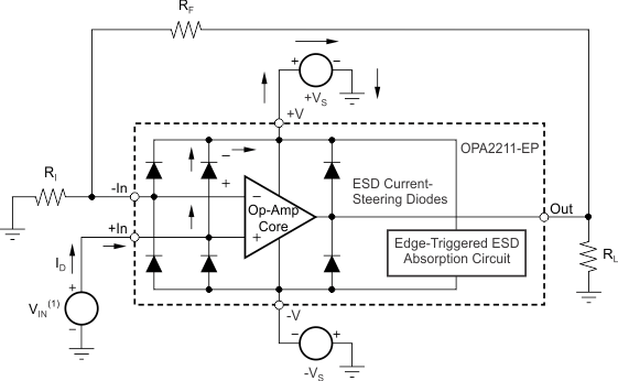
Figure 40 depicts a specific example where the input voltage, VIN, exceeds the positive supply voltage (+VS) by 500mV or more. Much of what happens in the circuit depends on the supply characteristics. If +VS can sink the current, one of the upper input steering diodes conducts and directs current to +VS. Excessively high current levels can flow with increasingly higher VIN. As a result, the data sheet specifications recommend that applications limit the input current to 10mA.
If the supply is not capable of sinking the current, VIN may begin sourcing current to the operational amplifier, and then take over as the source of positive supply voltage. The danger in this case is that the voltage can rise to levels that exceed the operational amplifier absolute maximum ratings. In extreme but rare cases, the absorption device triggers on while +VS and –VS are applied. If this event happens, a direct current path is established between the +VS and –VS supplies. The power dissipation of the absorption device is quickly exceeded, and the extreme internal heating destroys the operational amplifier.
Another common question involves what happens to the amplifier if an input signal is applied to the input while the power supplies +VS and/or –VS are at 0 V. Again, it depends on the supply characteristic while at 0V, or at a level below the input signal amplitude. If the supplies appear as high impedance, then the operational amplifier supply current may be supplied by the input source via the current steering diodes. This state is not a normal bias condition; the amplifier most likely will not operate normally. If the supplies are low impedance, then the current through the steering diodes can become quite high. The current level depends on the ability of the input source to deliver current, and any resistance in the input path.
8.2 Typical Application
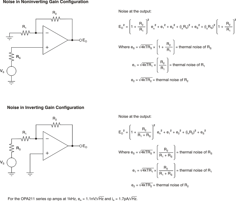 Figure 41. Noise Calculation in Gain Configurations
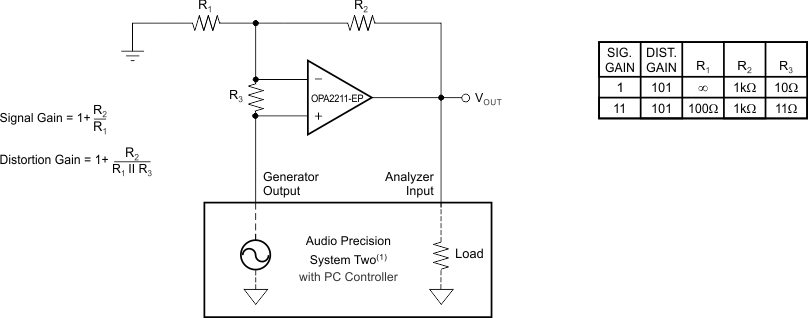 Figure 42. Distortion Test Circuit
8.2.1 Design Requirements
The design requirements for Signal Gain = 11 are:

where
- Supply voltage: 30 V (±15 V)
- R1 = 100 Ω
- R2 = 1 kΩ
- R3 = 11 Ω
8.2.2 Detailed Design Procedure
8.2.2.1 Total Harmonic Distortion Measurements
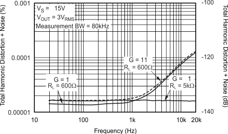
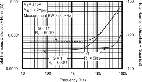
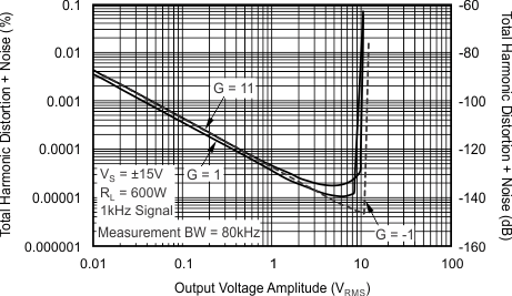
OPA2211-EP series operational amplifiers have excellent distortion characteristics. THD + Noise is below 0.0002% (G = +1, VOUT = 3VRMS) throughout the audio frequency range, 20 Hz to 20 kHz, with a 600-Ω load. The distortion produced by OPA2211-EP series operational amplifiers is below the measurement limit of many commercially available distortion analyzers. However, a special test circuit illustrated in Figure 47 can be used to extend the measurement capabilities.
Operational amplifier distortion can be considered an internal error source that can be referred to the input. Figure 47 shows a circuit that causes the operational amplifier distortion to be 101 times greater than that normally produced by the operational amplifier. The addition of R3 to the otherwise standard noninverting amplifier configuration alters the feedback factor or noise gain of the circuit. The closed-loop gain is unchanged, but the feedback available for error correction is reduced by a factor of 101, thus extending the resolution by 101. Note that the input signal and load applied to the operational amplifier are the same as with conventional feedback without R3. The value of R3 should be kept small to minimize its effect on the distortion measurements.
Validity of this technique can be verified by duplicating measurements at high gain and/or high frequency where the distortion is within the measurement capability of the test equipment. Measurements for this data sheet were made with an Audio Precision System Two distortion/noise analyzer, which greatly simplifies such repetitive measurements. The measurement technique can, however, be performed with manual distortion measurement instruments.
8.2.3 Application Curves
