ZHCSJ37 December 2018 OPA2313-Q1
PRODUCTION DATA.
7.3.5 Capacitive Load and Stability
The OPA2313-Q1 device is designed to be used in applications where driving a capacitive load is required. As with all op amps, there may be specific instances where the OPA2313-Q1 device may become unstable. The particular op amp circuit configuration, layout, gain, and output loading are some of the factors to consider when establishing whether or not an amplifier is stable in operation. An op amp in the unity-gain (+1-V/V) buffer configuration that drives a capacitive load exhibits a greater tendency to be unstable than an amplifier operated at a higher noise gain. The capacitive load, in conjunction with the op amp output resistance, creates a pole within the feedback loop that degrades the phase margin. The degradation of the phase margin increases as the capacitive loading increases. When operating in the unity-gain configuration, the OPA2313-Q1 device remains stable with a pure capacitive load up to approximately 1 nF. The equivalent series resistance (ESR) of some capacitors (CL greater than 1 µF) is sufficient to alter the phase characteristics in the feedback loop such that the amplifier remains stable. Increasing the amplifier closed-loop gain allows the amplifier to drive increasingly larger capacitance. This increased capability is evident when observing the overshoot response of the amplifier at higher voltage gains. See the typical characteristic graph, Figure 20.
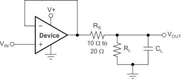
One technique for increasing the capacitive load drive capability of the amplifier when it operates in a unity-gain configuration is to insert a small resistor, typically 10 Ω to 20 Ω, in series with the output, as shown in Figure 34. This resistor significantly reduces the overshoot and ringing associated with large capacitive loads. One possible problem with this technique is that a voltage divider is created with the added series resistor and any resistor connected in parallel with the capacitive load. The voltage divider introduces a gain error at the output that reduces the output swing.
 Figure 34. Improving Capacitive Load Drive