ZHCSCS6B September   2014  – December 2018 OPA2320-Q1 , OPA320-Q1

PRODUCTION DATA.  

  1. 特性
  2. 应用
  3. 说明
    1.     零交叉失真:低偏移电压
  4. 修订历史记录
  5. Pin Configuration and Functions
    1.     Pin Functions
  6. Specifications
    1. 6.1 Absolute Maximum Ratings
    2. 6.2 ESD Ratings
    3. 6.3 Recommended Operating Conditions
    4. 6.4 Thermal Information
    5. 6.5 Electrical Characteristics:
    6. 6.6 Typical Characteristics
  7. Detailed Description
    1. 7.1 Overview
    2. 7.2 Functional Block Diagram
    3. 7.3 Feature Description
      1. 7.3.1 Input and ESD Protection
      2. 7.3.2 Feedback Capacitor Improves Response
      3. 7.3.3 EMI Susceptibility And Input Filtering
      4. 7.3.4 Output Impedance
      5. 7.3.5 Capacitive Load and Stability
      6. 7.3.6 Overload Recovery Time
    4. 7.4 Device Functional Modes
      1. 7.4.1 Rail-to-Rail Input
      2. 7.4.2 Phase Reversal
  8. Application and Implementation
    1. 8.1 Application Information
    2. 8.2 Typical Applications
      1. 8.2.1 Transimpedance Amplifier
        1. 8.2.1.1 Design Requirements
        2. 8.2.1.2 Detailed Design Procedure
          1. 8.2.1.2.1 Optimizing The Transimpedance Circuit
        3. 8.2.1.3 Application Curves
      2. 8.2.2 High-Impedance Sensor Interface
      3. 8.2.3 Driving ADCs
      4. 8.2.4 Active Filter
  9. Power Supply Recommendations
  10. 10Layout
    1. 10.1 Layout Guidelines
    2. 10.2 Layout Example
  11. 11器件和文档支持
    1. 11.1 器件支持
      1. 11.1.1 开发支持
    2. 11.2 相关链接
    3. 11.3 接收文档更新通知
    4. 11.4 社区资源
    5. 11.5 商标
    6. 11.6 静电放电警告
    7. 11.7 术语表
  12. 12机械、封装和可订购信息

封装选项

机械数据 (封装 | 引脚)
散热焊盘机械数据 (封装 | 引脚)
订购信息

Feedback Capacitor Improves Response

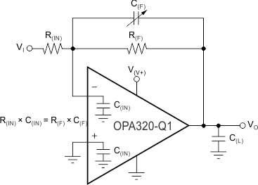
For optimum settling time and stability with high-impedance feedback networks, adding a feedback capacitor across the feedback resistor, R(FB), as shown in Figure 30 may be necessary. This capacitor compensates for the zero created by the feedback network impedance and the OPAx320-Q1 input capacitance (and any parasitic layout capacitance). The effect becomes more significant with higher impedance networks.
OPA320-Q1 OPA2320-Q1 ai_fback_dyna_perf_slos884.gif

NOTE:

Where C(IN) is equal to the OPAx320-Q1 input capacitance (approximately 9 pF) plus any parasitic layout capacitance.
Figure 30. Feedback Capacitor Improves Dynamic Performance

It is suggested that a variable capacitor be used for the feedback capacitor because input capacitance may vary between op amps and layout capacitance is difficult to determine. For the circuit shown in Figure 30, the value of the variable feedback capacitor should be chosen so that the input resistance times the input capacitance of the OPAx320-Q1 (9 pF, typical) plus the estimated parasitic layout capacitance equals the feedback capacitor times the feedback resistor:

Equation 1. R(IN) × C(IN) = R(FB) × C(FB)

where

  • C(IN) is equal to the OPAx320-Q1 input capacitance (sum of differential and common-mode) plus the layout capacitance.

The capacitor value can be adjusted until optimum performance is obtained.