SBOS483I July 2009 – May 2015 OPA2333-HT
PRODUCTION DATA.
- 1 Features
- 2 Applications
- 3 Description
- 4 Revision History
- 5 Pin Configuration and Functions
- 6 Specifications
- 7 Detailed Description
- 8 Application and Implementation
- 9 Power Supply Recommendations
- 10Layout
- 11Device and Documentation Support
- 12Mechanical, Packaging, and Orderable Information
封装选项
机械数据 (封装 | 引脚)
散热焊盘机械数据 (封装 | 引脚)
订购信息
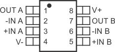
5 Pin Configuration and Functions
D, JD, or HKJ Package
8-Pin SOIC, CDIP SB, or CFP
Top View

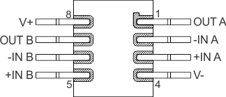
HKQ Package
8-Pin CFP
Top View

HKQ as formed or HKL mounted dead bug
Pin Functions
| PIN | I/O | DESCRIPTION | |
|---|---|---|---|
| NO. | NAME | ||
| 1 | OUT A | O | Analog output channel A |
| 2 | –IN A | I | Inverting analog input channel A |
| 3 | +IN A | I | Noninverting analog input channel A |
| 5 | +IN B | I | Noninverting analog input channel B |
| 6 | –IN B | I | Inverting analog input channel B |
| 4 | V– | — | Negative (lowest) power supply |
| 7 | OUT B | O | Analog output channel B |
| 8 | V+ | — | Positive (highest) power supply |

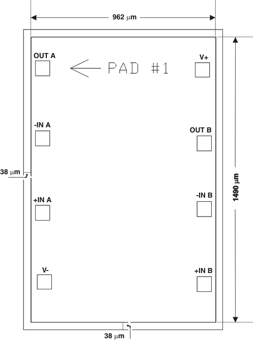
Table 1. Bare Die Information
| DIE THICKNESS | BACKSIDE FINISH | BACKSIDE POTENTIAL |
BOND PAD METALLIZATION COMPOSITION |
|---|---|---|---|
| 15 mils. | Silicon with backgrind | V- | Al-Si-Cu (0.5%) |
Table 2. Bond Pad Coordinates
| DESCRIPTION | PAD NUMBER | A | B | C | D |
|---|---|---|---|---|---|
| OUT A | 1 | 21.20 | 1288.50 | 97.20 | 1364.50 |
| –IN A | 2 | 21.20 | 923.65 | 97.20 | 999.65 |
| +IN A | 3 | 21.20 | 533.05 | 97.20 | 609.05 |
| V– | 4 | 31.30 | 172.20 | 107.30 | 248.20 |
| +IN B | 5 | 864.80 | 162.25 | 940.80 | 238.25 |
| –IN B | 6 | 864.80 | 552.65 | 940.80 | 628.65 |
| OUT B | 7 | 864.80 | 897.10 | 940.80 | 973.10 |
| V+ | 8 | 854.70 | 1280.45 | 930.70 | 1356.45 |