SBOS073C September 1997 – August 2016 OPA2340 , OPA340 , OPA4340
PRODUCTION DATA.
- 1 Features
- 2 Applications
- 3 Description
- 4 Revision History
- 5 Pin Configuration and Functions
- 6 Specifications
- 7 Detailed Description
- 8 Application and Implementation
- 9 Power Supply Recommendations
- 10Layout
- 11Device and Documentation Support
- 12Mechanical, Packaging, and Orderable Information
封装选项
机械数据 (封装 | 引脚)
散热焊盘机械数据 (封装 | 引脚)
订购信息
6 Specifications
6.1 Absolute Maximum Ratings
over operating free-air temperature range (unless otherwise noted)(1)| MIN | MAX | UNIT | |||
|---|---|---|---|---|---|
| Voltage | Supply voltage | 5.5 | V | ||
| Signal input terminals(2) | –0.5 | 0.5 | |||
| Current | Signal input terminals(2) | 10 | mA | ||
| Output short circuit(3) | Continuous | ||||
| Temperature | Operating, TA | –55 | 125 | °C | |
| Junction, TJ | 150 | ||||
| Storage, Tstg | –55 | 125 | |||
(1) Stresses beyond those listed under Absolute Maximum Ratings may cause permanent damage to the device. These are stress ratings only, which do not imply functional operation of the device at these or any other conditions beyond those indicated under Recommended Operating Conditions. Exposure to absolute-maximum-rated conditions for extended periods may affect device reliability.
(2) Input terminals are diode-clamped to the power-supply rails. Input signals that can swing more than 0.5 V beyond the supply rails should be current limited to 10 mA or less.
(3) Short-circuit to ground, one amplifier per package.
6.2 ESD Ratings
| VALUE | UNIT | |||
|---|---|---|---|---|
| V(ESD) | Electrostatic discharge | Human-body model (HBM), per ANSI/ESDA/JEDEC JS-001(1) | ±600 | V |
| Charged-device model (CDM), per JEDEC specification JESD22-C101(2) | ±250 | |||
(1) JEDEC document JEP155 states that 500-V HBM allows safe manufacturing with a standard ESD control process.
(2) JEDEC document JEP157 states that 250-V CDM allows safe manufacturing with a standard ESD control process.
6.3 Recommended Operating Conditions
over operating free-air temperature range (unless otherwise noted)| MIN | MAX | UNIT | ||
|---|---|---|---|---|
| Supply voltage | 2.7 | 5.5 | V | |
| Specified temperature | –40 | 125 | °C | |
6.4 Thermal Information – OPA340
| THERMAL METRIC(1) | OPA340 | UNIT | ||||
|---|---|---|---|---|---|---|
| DBV (SOT-23) |
P (PDIP) |
D (SOIC) |
D (SOIC) |
|||
| 5 PINS | 8 PINS | 8 PINS | 14 PINS | |||
| RθJA | Junction-to-ambient thermal resistance | 207.9 | 53.1 | 142 | 83.8 | °C/W |
| RθJC(top) | Junction-to-case (top) thermal resistance | 71.2 | 42.5 | 90.2 | 70.7 | °C/W |
| RθJB | Junction-to-board thermal resistance | 36.0 | 30.3 | 82.5 | 59.5 | °C/W |
| ψJT | Junction-to-top characterization parameter | 2.0 | 19.7 | 39.4 | 11.6 | °C/W |
| ψJB | Junction-to-board characterization parameter | 35.2 | 30.2 | 82 | 37.7 | °C/W |
| RθJC(bot) | Junction-to-case (bottom) thermal resistance | — | — | — | — | °C/W |
(1) For more information about traditional and new thermal metrics, see the Semiconductor and IC Package Thermal Metrics application report.
6.5 Thermal Information – OPA2340
| THERMAL METRIC(1) | OPA2340 | UNIT | ||
|---|---|---|---|---|
| D (SOIC) |
DGK (VSSOP) |
|||
| 8 PINS | 8 PINS | |||
| RθJA | Junction-to-ambient thermal resistance | 138.4 | 169.2 | °C/W |
| RθJC(top) | Junction-to-case (top) thermal resistance | 89.5 | 62.8 | °C/W |
| RθJB | Junction-to-board thermal resistance | 78.6 | 89.8 | °C/W |
| ψJT | Junction-to-top characterization parameter | 29.9 | 7.5 | °C/W |
| ψJB | Junction-to-board characterization parameter | 78.1 | 88.2 | °C/W |
| RθJC(bot) | Junction-to-case (bottom) thermal resistance | — | — | °C/W |
(1) For more information about traditional and new thermal metrics, see the Semiconductor and IC Package Thermal Metrics application report.
6.6 Thermal Information – OPA4340
| THERMAL METRIC(1) | OPA4340 | UNIT | |
|---|---|---|---|
| DBQ (SSOP) |
|||
| 16 PINS | |||
| RθJA | Junction-to-ambient thermal resistance | 115.8 | °C/W |
| RθJC(top) | Junction-to-case (top) thermal resistance | 67 | °C/W |
| RθJB | Junction-to-board thermal resistance | 58.3 | °C/W |
| ψJT | Junction-to-top characterization parameter | 19.9 | °C/W |
| ψJB | Junction-to-board characterization parameter | 57.9 | °C/W |
| RθJC(bot) | Junction-to-case (bottom) thermal resistance | — | °C/W |
(1) For more information about traditional and new thermal metrics, see the Semiconductor and IC Package Thermal Metrics application report.
6.7 Electrical Characteristics
At TA = 25°C, RL = 10 kΩ connected to VS/2, and VOUT = VS/2, unless otherwise noted.| PARAMETER | TEST CONDITIONS | MIN | TYP(1) | MAX | UNIT | ||
|---|---|---|---|---|---|---|---|
| OFFSET VOLTAGE | |||||||
| VOS | Input offset voltage | VS = 5 V | ±150 | ±500 | µV | ||
| dVOS/dt | Input offset voltage vs temperature | TA = –40°C to 85°C, VS = 5 V | ±2.5 | µV/°C | |||
| PSRR | Input offset voltage vs power supply | VS = 2.7 V to 5.5 V, VCM = 0 V | 30 | 120 | µV/V | ||
| Over temperature | VS = 2.7 V to 5.5 V, VCM = 0 V, TA = –40°C to 85°C, VS = 5 V |
120 | µV/°C | ||||
| Channel separation, DC | 0.2 | µV/V | |||||
| INPUT BIAS CURRENT | |||||||
| IS | Input bias current | ±0.2 | ±10 | pA | |||
| Over temperature | TA = –40°C to 85°C, VS = 5 V | ±60 | |||||
| IOS | Input offset current | ±0.2 | ±10 | pA | |||
| NOISE | |||||||
| Input voltage noise | f = 0.1 kHz to 50 kHz | 8 | µVRMS | ||||
| en | Input voltage noise density | f = 1 kHz | 25 | nV/√Hz | |||
| in | Current noise density | f = 1 kHz | 3 | fA/√Hz | |||
| INPUT VOLTAGE RANGE | |||||||
| VCM | Common-mode voltage range | –0.3 | (V+) + 0.3 | V | |||
| CMRR | Common-mode rejection ratio | –0.3 V < VCM < (V+) – 1.8 V | 80 | 92 | dB | ||
| VS = 5 V, –0.3 V < VCM < 5.3 V | 70 | 84 | |||||
| VS = 2.7 V, –0.3 V < VCM < 3 V | 66 | 80 | |||||
| INPUT IMPEDANCE | |||||||
| Differential | 1013 || 3 | Ω || pF | |||||
| Common-mode | 1013 || 6 | Ω || pF | |||||
| OPEN-LOOP GAIN | |||||||
| AOL | Open-loop voltage gain | RL = 100 kΩ, 5 mV < VO < (V+) – 5 mV |
106 | 124 | dB | ||
| RL = 10 kΩ, 5 mV < VO < (V+) – 50 mV |
100 | 120 | |||||
| RL = 2 kΩ, 200 mV < VO < (V+) – 200 mV |
94 | 114 | |||||
| Over temperature | RL = 100 kΩ, 5 mV < VO < (V+) – 5 mV, TA = –40°C to 85°C, VS = 5 V |
106 | |||||
| RL = 10 kΩ, 5 mV < VO < (V+) – 50 mV, TA = –40°C to 85°C, VS = 5 V |
100 | ||||||
| RL = 2 kΩ, 200 mV < VO < (V+) – 200 mV, TA = –40°C to 85°C, VS = 5 V |
94 | ||||||
| FREQUENCY RESPONSE | |||||||
| GBW | Gain-bandwidth product | G = 1 | 5.5 | MHz | |||
| SR | Slew rate | VS = 5 V, G = 1, CL = 100 pF | 6 | V/µs | |||
| Settling time, 0.1% | VS = 5 V, 2-V step, CL = 100 pF | 1 | µs | ||||
| Settling time, 0.01% | VS = 5 V, 2-V step, CL = 100 pF | 1.6 | µs | ||||
| Overload recovery time | VIN × G = VS | 0.2 | µs | ||||
| THD+N | Total harmonic distortion + noise | VS = 5 V, VO = 3VPP(2), G = 1, f = 1 kHz |
0.0007% | ||||
| OUTPUT | |||||||
| Voltage output swing from rail(2) | RL = 100 kΩ, AOL ≥ 106 dB | 1 | 5 | mV | |||
| RL = 10 kΩ, AOL ≥ 106 dB | 10 | ||||||
| RL = 2 kΩ, AOL ≥ 106 dB | 40 | ||||||
| Over temperature | RL = 100 kΩ, AOL ≥ 106 dB, TA = –40°C to 85°C, VS = 5 V |
5 | |||||
| RL = 10 kΩ, AOL ≥ 106 dB, TA = –40°C to 85°C, VS = 5 V |
50 | ||||||
| RL = 2 kΩ, AOL ≥ 106 dB, TA = –40°C to 85°C, VS = 5 V |
200 | ||||||
| ISC | Short-circuit current | ±50 | mA | ||||
| CLOAD | Capacitive load drive | See Typical Characteristics | |||||
| POWER SUPPLY | |||||||
| VS | Specified voltage range | 2.7 | 5 | V | |||
| Operating voltage range | Lower end | 2.5 | V | ||||
| Higher end | 5.5 | ||||||
| IQ | Quiescent current (per amplifier) |
IO = 0, VS = 5 V | 750 | 950 | µA | ||
| Over temperature | IO = 0, VS = 5 V, TA = –40°C to 85°C | 100 | |||||
| TEMPERATURE RANGE | |||||||
| Specified range | –40 | 85 | °C | ||||
| Operating range | –55 | 125 | °C | ||||
| Storage range | –55 | 125 | °C | ||||
(1) VS = 5 V.
(2) Output voltage swings are measured between the output and power-supply rails.
6.8 Typical Characteristics
At TA = 25°C, VS = 5 V, and RL = 10 kΩ connected to VS/2, unless otherwise noted. Figure 1. Open-Loop Gain/Phase vs Frequency
 Figure 3. Input Voltage and Current Noise Spectral Density vs Frequency
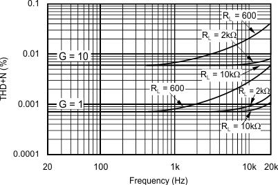 Figure 5. Total Harmonic Distortion + Noise vs Frequency
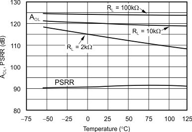 Figure 7. Open-Loop Gain and Power-Supply Rejection vs Temperature
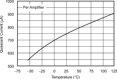 Figure 9. Quiescent Current vs Temperature
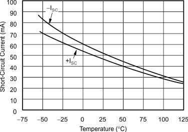 Figure 11. Short-Circuit Current vs Temperature
 Figure 13. Input Bias Current vs Temperature
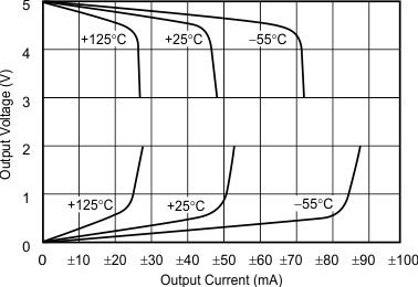 Figure 15. Output Voltage Swing vs Output Current
 Figure 17. Offset Voltage Production Distribution
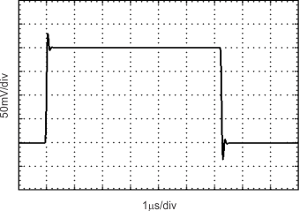
| CL = 100 pF |
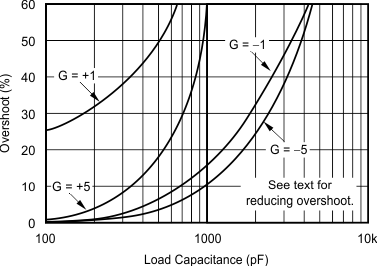 Figure 21. Small-Signal Overshoot vs Load Capacitance
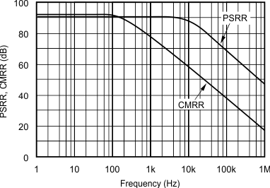 Figure 2. Power-Supply and Common-Mode Rejection vs Frequency
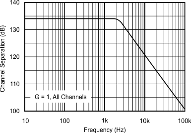 Figure 4. Channel Separation vs Frequency
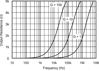 Figure 6. Closed-Loop Output Impedance vs Frequency
 Figure 8. Common-Mode Rejection vs Temperature
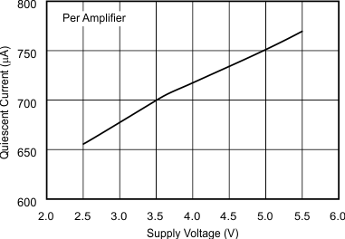 Figure 10. Quiescent Current vs Supply Voltage
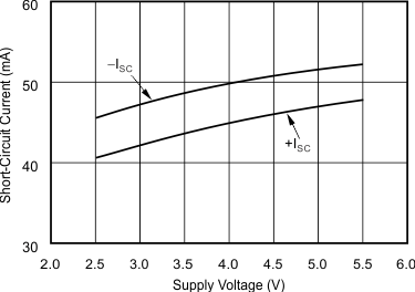 Figure 12. Short-Circuit Current vs Supply Voltage
 Figure 14. Input Bias Current vs Input Common-Mode Voltage
 Figure 16. Maximum Output Voltage vs Frequency
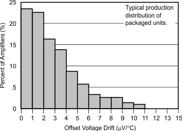 Figure 18. Offset Voltage Drift Magnitude Production Distribution
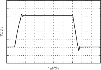
| CL = 100 pF |
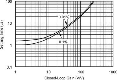 Figure 22. Settling Time vs Closed-Loop Gain