ZHCSI30G March 2002 – April 2018 OPA2354 , OPA354 , OPA4354
PRODUCTION DATA.
- 1 特性
- 2 应用
- 3 说明
- 4 修订历史记录
- 5 Device Comparison Table
- 6 Pin Configuration and Functions
- 7 Specifications
- 8 Detailed Description
- 9 Application and Implementation
- 10Power Supply Recommendations
- 11Layout
- 12器件和文档支持
- 13机械、封装和可订购信息
封装选项
机械数据 (封装 | 引脚)
散热焊盘机械数据 (封装 | 引脚)
- DDA|8
订购信息
8.3.7 Capacitive Load and Stability
The OPAx354 series op amps drives a wide range of capacitive loads. However, all op amps may become unstable under certain conditions. Op amp configuration, gain, and load value are just a few of the factors to consider when determining stability. An op amp in unity-gain configuration is most susceptible to the effects of capacitive loading. The capacitive load reacts with the device output resistance, along with any additional load resistance, to create a pole in the small-signal response that degrades the phase margin. See the Frequency Response for Various CL typical characteristic curve (Figure 13) for details.
The OPAx354 topology enhances its ability to drive capacitive loads. In unity gain, these op amps perform well with large capacitive loads. See the Recommended RS vs Capacitive Load (Figure 14) and Frequency Response vs Capacitive Load (Figure 15) typical characteristic curves for details.
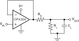
One method of improving capacitive load drive in the unity-gain configuration is to insert a 10-Ω to 20-Ω resistor in series with the output, as shown in Figure 35. This configuration significantly reduces ringing with large capacitive loads; see the Frequency Response vs Capacitive Load typical characteristic curve (Figure 15). However, if there is a resistive load in parallel with the capacitive load, RS creates a voltage divider. This voltage division introduces a DC error at the output and slightly reduces output swing. This error may be insignificant. For instance, with RL = 10 kΩ and RS = 20 Ω, there is an error of approximately 0.2% at the output.
 Figure 35. Series Resistor in Unity-Gain Configuration Improves Capacitive Load Drive