ZHCSJD6 February   2019 OPA2356-EP

PRODUCTION DATA.  

  1. 特性
  2. 应用
  3. 说明
    1.     Device Images
      1.      简化原理图
  4. 修订历史记录
  5. Pin Configuration and Functions
    1.     Pin Functions
  6. Specifications
    1. 6.1 Absolute Maximum Ratings
    2. 6.2 ESD Ratings
    3. 6.3 Recommended Operating Conditions
    4. 6.4 Thermal Information
    5. 6.5 Electrical Characteristics
    6. 6.6 Typical Characteristics
  7. Detailed Description
    1. 7.1 Overview
    2. 7.2 Functional Block Diagram
    3. 7.3 Feature Description
      1. 7.3.1 Operating Voltage
      2. 7.3.2 Output Drive
    4. 7.4 Device Functional Modes
  8. Application and Implementation
    1. 8.1 Application Information
    2. 8.2 Typical Applications
      1. 8.2.1 Transimpedance Amplifier
        1. 8.2.1.1 Design Requirements
        2. 8.2.1.2 Detailed Design Procedure
          1. 8.2.1.2.1 Custom Design With WEBENCH® Tools
          2. 8.2.1.2.2 OPA2356-EP Design Procedure
            1. 8.2.1.2.2.1 Optimizing the Transimpedance Circuit
        3. 8.2.1.3 Application Curve
      2. 8.2.2 High-Impedance Sensor Interface
      3. 8.2.3 Driving ADCs
      4. 8.2.4 Active Filter
  9. Power Supply Recommendations
  10. 10Layout
    1. 10.1 Layout Guidelines
    2. 10.2 Layout Example
  11. 11器件和文档支持
    1. 11.1 文档支持
      1. 11.1.1 相关文档
    2. 11.2 接收文档更新通知
    3. 11.3 社区资源
    4. 11.4 商标
    5. 11.5 静电放电警告
    6. 11.6 术语表
  12. 12机械、封装和可订购信息

封装选项

机械数据 (封装 | 引脚)
散热焊盘机械数据 (封装 | 引脚)
订购信息

Transimpedance Amplifier

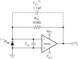
Wide gain bandwidth, low input bias current, low input voltage, and current noise make the OPA2356-EP a preferred wideband photodiode transimpedance amplifier. Low-voltage noise is important because photodiode capacitance causes the effective noise gain of the circuit to increase at high frequency.

The key elements to a transimpedance design, as shown in Figure 30, are the expected diode capacitance (C(D)), which must include the parasitic input common-mode and differential-mode input capacitance (4 pF + 5 pF), the desired transimpedance gain (R(FB)), and the gain-bandwidth (GBW) for the OPA2356-EP (20 MHz). With these three variables set, the feedback capacitor value (C(FB)) is set to control the frequency response. C(FB) includes the stray capacitance of R(FB), which is 0.2 pF for a typical surface-mount resistor.
OPA2356-EP ai_trans_amp_dual_sbos212.gif
C(FB) is optional to prevent gain peaking. C(FB) includes the stray capacitance of R(FB).
Figure 30. Dual-Supply Transimpedance Amplifier