ZHCSJD6 February 2019 OPA2356-EP
PRODUCTION DATA.
- 1 特性
- 2 应用
- 3 说明
- 4 修订历史记录
- 5 Pin Configuration and Functions
- 6 Specifications
- 7 Detailed Description
- 8 Application and Implementation
- 9 Power Supply Recommendations
- 10Layout
- 11器件和文档支持
- 12机械、封装和可订购信息
8.2.2 High-Impedance Sensor Interface
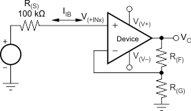
Many sensors have high source impedances that may range up to 10 MΩ, or even higher. The output signal of sensors often must be amplified or otherwise conditioned by means of an amplifier. The input bias current of this amplifier can load the sensor output and cause a voltage drop across the source resistance, as shown in Figure 33, where (V(+INx) = VS – I(BIAS) × R(S)). The last term, I(BIAS) × R(S), shows the voltage drop across R(S). To prevent errors introduced to the system as a result of this voltage, an op amp with very low input bias current must be used with high impedance sensors. This low current keeps the error contribution by I(BIAS) × R(S) less than the input voltage noise of the amplifier, so that the input voltage noise does not become the dominant noise factor. The OPA2356-EP op amp features very low input bias current (typically 200 fA) and is therefore a preferred choice for such applications.
 Figure 33. Noise as a Result of I(BIAS)