ZHCSI16F March   2002  – April 2018 OPA2357 , OPA357

PRODUCTION DATA.  

  1. 特性
  2. 应用
  3. 说明
    1.     Device Images
      1.      简化原理图
  4. 修订历史记录
  5. Pin Configuration and Functions
    1.     Pin Functions
  6. Specifications
    1. 6.1 Absolute Maximum Ratings
    2. 6.2 ESD Ratings
    3. 6.3 Recommended Operating Conditions
    4. 6.4 Thermal Information
    5. 6.5 Electrical Characteristics: VS = +2.7-V to +5.5-V Single-Supply
    6. 6.6 Typical Characteristics
  7. Detailed Description
    1. 7.1 Overview
    2. 7.2 Functional Block Diagram
    3. 7.3 Feature Description
      1. 7.3.1  OPAx357 Comparison
      2. 7.3.2  Operating Voltage
      3. 7.3.3  Enable Function
      4. 7.3.4  Rail-to-Rail Input
      5. 7.3.5  Rail-to-Rail Output
      6. 7.3.6  Output Drive
      7. 7.3.7  Video
      8. 7.3.8  Wideband Video Multiplexing
      9. 7.3.9  Driving Analog-to-Digital Converters
      10. 7.3.10 Capacitive Load and Stability
      11. 7.3.11 Wideband Transimpedance Amplifier
    4. 7.4 Device Functional Modes
  8. Application and Implementation
    1. 8.1 Application Information
    2. 8.2 Typical Applications
      1. 8.2.1 Transimpedance Amplifier
        1. 8.2.1.1 Design Requirements
        2. 8.2.1.2 Detailed Design Procedure
          1. 8.2.1.2.1 Custom Design With WEBENCH® Tools
          2. 8.2.1.2.2 OPAx357 Design Procedure
            1. 8.2.1.2.2.1 Optimizing the Transimpedance Circuit
        3. 8.2.1.3 Application Curve
      2. 8.2.2 High-Impedance Sensor Interface
      3. 8.2.3 Driving ADCs
      4. 8.2.4 Active Filter
  9. Power Supply Recommendations
    1. 9.1 Power Dissipation
  10. 10Layout
    1. 10.1 Layout Guidelines
    2. 10.2 Layout Example
  11. 11器件和文档支持
    1. 11.1 器件支持
      1. 11.1.1 开发支持
        1. 11.1.1.1 使用 WEBENCH® 工具创建定制设计
    2. 11.2 文档支持
      1. 11.2.1 相关文档
    3. 11.3 相关链接
    4. 11.4 接收文档更新通知
    5. 11.5 社区资源
    6. 11.6 商标
    7. 11.7 静电放电警告
    8. 11.8 Glossary
  12. 12机械、封装和可订购信息

封装选项

机械数据 (封装 | 引脚)
散热焊盘机械数据 (封装 | 引脚)
订购信息

Typical Characteristics

at TA = 25°C, VS = 5 V, G = +1, RF = 0 Ω, RL = 1 kΩ, and connected to VS / 2 (unless otherwise noted)
OPA357 OPA2357 OPA357_SBOS235_G001.gif
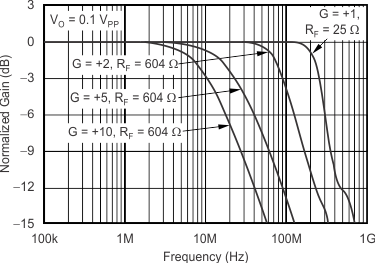
Figure 1. Noninverting Small-Signal Frequency Response
OPA357 OPA2357 OPA357_SBOS235_G003.gif
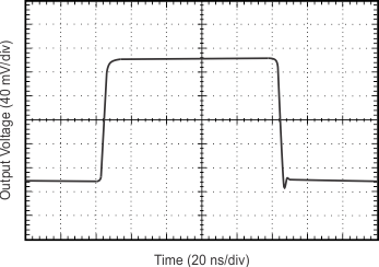
Figure 3. Noninverting Small-Signal Step Response
OPA357 OPA2357 OPA357_SBOS235_G005.gif
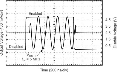
Figure 5. Large-Signal Disable, Enable Response
OPA357 OPA2357 OPA357_SBOS235_G007.gif
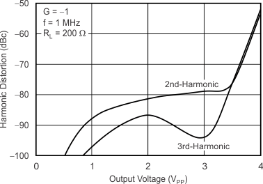
Figure 7. Harmonic Distortion vs Output Voltage
OPA357 OPA2357 OPA357_SBOS235_G009.gif
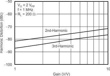
Figure 9. Harmonic Distortion vs Inverting Gain
OPA357 OPA2357 OPA357_SBOS235_G011.gif
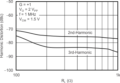
Figure 11. Harmonic Distortion vs Load Resistance
OPA357 OPA2357 OPA357_SBOS235_G013.gif
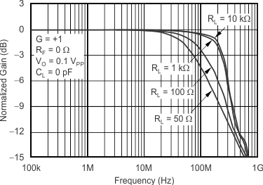
Figure 13. Frequency Response for Various RL
OPA357 OPA2357 OPA357_SBOS235_G015.gif
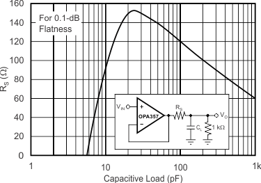
Figure 15. Recommended RS vs Capacitive Load
OPA357 OPA2357 OPA357_SBOS235_G017.gif
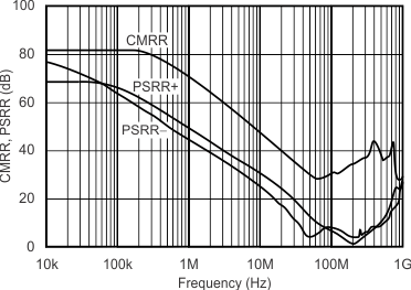
Figure 17. Common-Mode Rejection Ratio and Power-Supply Rejection Ratio vs Frequency
OPA357 OPA2357 OPA357_SBOS235_G019.gif
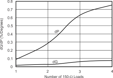
Figure 19. Composite Video differential Gain and Phase
OPA357 OPA2357 OPA357_SBOS235_G021.gif
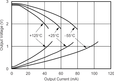
VS = 3 V
Figure 21. Output Voltage Swing vs Output Current
OPA357 OPA2357 OPA357_SBOS235_G023.gif
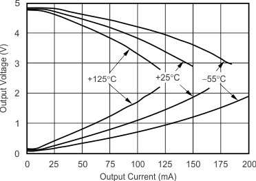
VS = 5 V
Figure 23. Output Voltage Swing vs Output Current
OPA357 OPA2357 OPA357_SBOS235_G025.gif
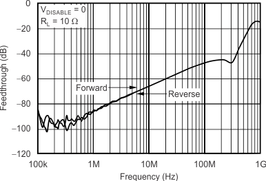
Figure 25. Disable Feedthrough vs Frequency
OPA357 OPA2357 OPA357_SBOS235_G027.gif
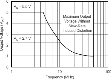
Figure 27. Maximum Output Voltage vs Frequency
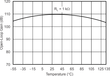
OPA357 OPA2357 OPA357_SBOS235_G029.gif
Figure 29. Open-Loop Gain vs Temperature
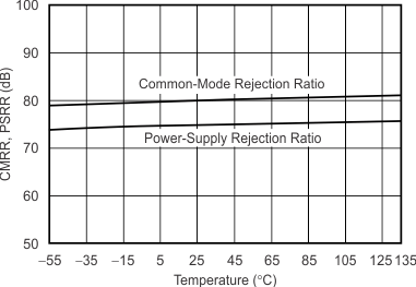
OPA357 OPA2357 OPA357_SBOS235_G031.gif
Figure 31. Common-Mode Rejection Ratio and Power-Supply Rejection Ratio vs Temperature
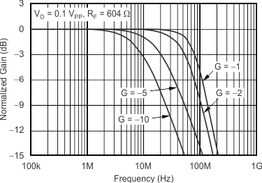
OPA357 OPA2357 OPA357_SBOS235_G002.gif
Figure 2. Inverting Small-Signal Frequency Response
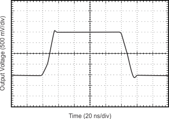
OPA357 OPA2357 OPA357_SBOS235_G004.gif
Figure 4. Noninverting Large-Signal Step Response
OPA357 OPA2357 OPA357_SBOS235_G006.gif
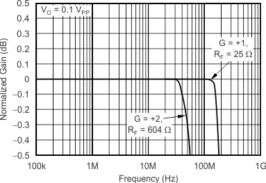
Figure 6. 0.1-dB Gain Flatness
OPA357 OPA2357 OPA357_SBOS235_G008.gif
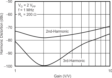
Figure 8. Harmonic Distortion vs Noninverting Gain
OPA357 OPA2357 OPA357_SBOS235_G010.gif
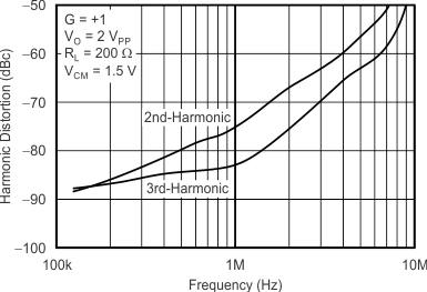
Figure 10. Harmonic Distortion vs Frequency
OPA357 OPA2357 OPA357_SBOS235_G012.gif
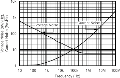
Figure 12. Input Voltage and Current Noise Spectral Density vs Frequency
OPA357 OPA2357 OPA357_SBOS235_G014.gif
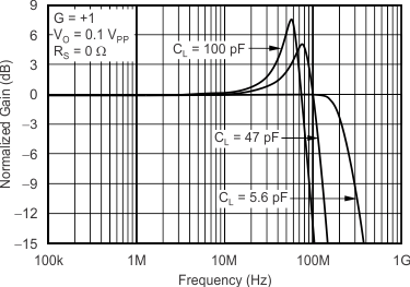
Figure 14. Frequency Response for Various CL
OPA357 OPA2357 OPA357_SBOS235_G016.gif
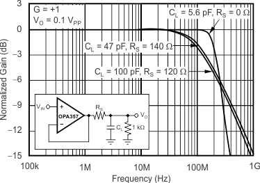
Figure 16. Frequency Response vs Capacitive Load
OPA357 OPA2357 OPA357_SBOS235_G018.gif
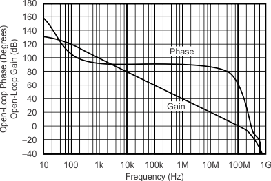
Figure 18. Open-Loop Gain and Phase
OPA357 OPA2357 OPA357_SBOS235_G020.gif
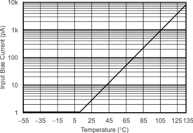
Figure 20. Input Bias Current vs Temperature
OPA357 OPA2357 OPA357_SBOS235_G022.gif
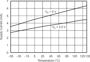
Figure 22. Supply Current vs Temperature
OPA357 OPA2357 OPA357_SBOS235_G024.gif
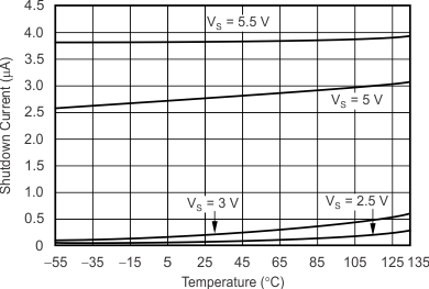
Figure 24. Shutdown Current vs Temperature
OPA357 OPA2357 OPA357_SBOS235_G026.gif
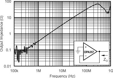
Figure 26. Closed-Loop Output Impedance vs Frequency
OPA357 OPA2357 OPA357_SBOS235_G028.gif
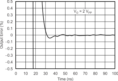
Figure 28. Output Settling Time to 0.1%
OPA357 OPA2357 OPA357_SBOS235_G030.gif
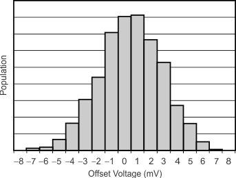
Figure 30. Offset Voltage Production Distribution
OPA357 OPA2357 OPA357_SBOS235_G032.gif
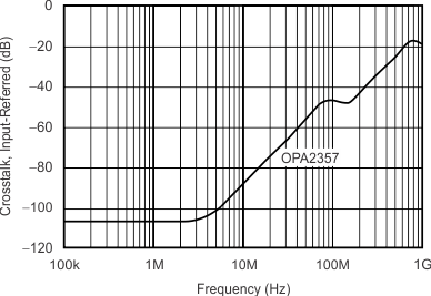
Figure 32. Channel-to-Channel Crosstalk