ZHCSNC5A February 2021 – April 2021 OPA2607-Q1 , OPA607-Q1
PRODUCTION DATA
- 1 特性
- 2 应用
- 3 说明
- 4 Revision History
- 5 Device Comparison
- 6 Pin Configuration and Functions
- 7 Specifications
- 8 Detailed Description
- 9 Application and Implementation
- 10Power Supply Recommendations
- 11Layout
- 12Device and Documentation Support
- 13Mechanical, Packaging, and Orderable Information
9.2.2 Noninverting Gain of 3 V/V
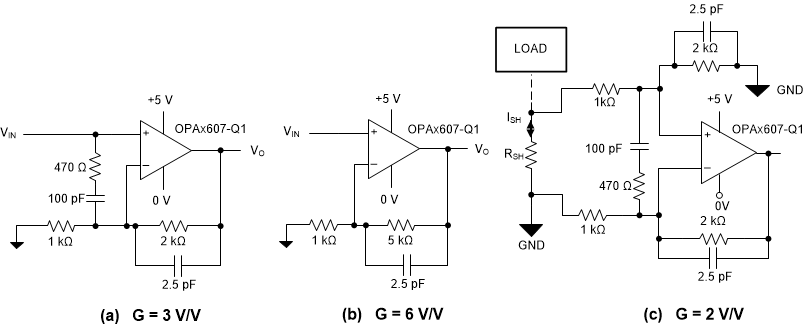
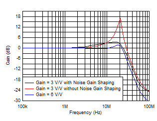
The OPAx607-Q1 devices are normally stable in noise gain configurations (see SBOA066) of greater than 6 V/V when conventional feedback networks are used, which is discussed in Section 8.3.4. The OPAx607-Q1 devices can be configured in noise gains of less than 6 V/V by using capacitors in the feedback path and between the inputs to maintain the desired gain at lower frequencies and increase the gain greater that 6 V/V at higher frequencies such that the amplifier is stable. Configuration (a) in Figure 9-6 shows OPAx607-Q1 devices configured in a gain of 3 V/V by using capacitors and resistors to shape the noise gain and achieve a phase margin of approximately 56° that is very close to the phase margin achieved for the conventional 6 V/V configuration (b) in Figure 9-6.
The key benefit of using a decompensated amplifier (such as the OPAx607-Q1) below the minimum stable gain, is that it takes advantage of the low noise and low distortion performance at quiescent powers smaller than comparable unity-gain stable architectures. By reducing the 100-pF input capacitor, higher closed-loop bandwidth can be achieved at the expense of increased peaking and reduced phase margin. Ensure that low parasitic capacitance layout techniques on the IN– pin are as small as 1 pF to 2 pF of parasitic capacitance on the inverting input, which will require tweaking the noise-shaping component values to get a flat frequency response and the desired phase margin. Configurations in Figure 9-6 does not take into account this parasitic capacitance but it must be considered for practical purposes. Details on the benefits of decompensated architectures are discussed in Using a decompensated op amp for improved performance. The one-capacitor, externally compensated type method is used for noise gain shaping in the below circuit.
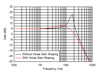
In a difference amplifier circuit, typically used for low side current sensing applications, the (noise gain) = (signal gain + 1).
 Figure 9-6 Noninverting Gain of 3 V/V, 6 V/V
Configurations, and Difference Amplifier in Signal Gain of 2 V/V
 Figure 9-7 Small-Signal Frequency Response in Gains of 3V/V (a) and 6V/V (b)
 Figure 9-8 Small-Signal Frequency Response of Difference Amplifier (c) With and
Without Noise Gain Shaping