ZHCSF85A July   2016  – December 2019 OPA2626

PRODUCTION DATA.  

  1. 特性
  2. 应用
  3. 说明
    1.     Device Images
      1.      SAR ADC 驱动器
      2.      高保真拓扑改善了动态性能 (fIN = 10kHz,1MSPS FFT)
  4. 修订历史记录
  5. Pin Configuration and Functions
    1.     Pin Functions: OPA2626
  6. Specifications
    1. 6.1 Absolute Maximum Ratings
    2. 6.2 ESD Ratings
    3. 6.3 Recommended Operating Conditions
    4. 6.4 Thermal Information
    5. 6.5 Electrical Characteristics: High-Supply
    6. 6.6 Electrical Characteristics: Low-Supply
    7. 6.7 Typical Characteristics
  7. Parameter Measurement Information
    1. 7.1 DC Parameter Measurements
    2. 7.2 Transient Parameter Measurements
    3. 7.3 AC Parameter Measurements
    4. 7.4 Noise Parameter Measurements
  8. Detailed Description
    1. 8.1 Overview
    2. 8.2 Functional Block Diagram
    3. 8.3 Feature Description
      1. 8.3.1 SAR ADC Driver
      2. 8.3.2 Electrical Overstress
    4. 8.4 Device Functional Modes
      1. 8.4.1 High-Drive Mode
  9. Application and Implementation
    1. 9.1 Application Information
    2. 9.2 Typical Applications
      1. 9.2.1 Single-Supply, 16-Bit, 1-MSPS SAR ADC Driver
        1. 9.2.1.1 Design Requirements
        2. 9.2.1.2 Detailed Design Procedure
        3. 9.2.1.3 Application Curve
      2. 9.2.2 Single-Supply, 16-Bit, 1-MSPS, Multiplexed, SAR ADC Driver
        1. 9.2.2.1 Design Requirements
        2. 9.2.2.2 Detailed Design Procedure
        3. 9.2.2.3 Application Curves
  10. 10Power Supply Recommendations
  11. 11Layout
    1. 11.1 Layout Guidelines
    2. 11.2 Layout Example
  12. 12器件和文档支持
    1. 12.1 器件支持
      1. 12.1.1 开发支持
        1. 12.1.1.1 TINA-TI(免费软件下载)
        2. 12.1.1.2 TI 高精度设计
    2. 12.2 文档支持
      1. 12.2.1 相关文档
    3. 12.3 接收文档更新通知
    4. 12.4 社区资源
    5. 12.5 商标
    6. 12.6 静电放电警告
    7. 12.7 Glossary
  13. 13机械、封装和可订购信息

封装选项

机械数据 (封装 | 引脚)
散热焊盘机械数据 (封装 | 引脚)
订购信息

Typical Characteristics

at TA = 25°C, V+ = 5 V, V– = 0 V, VCOM = VO = 2.5 V, gain (G) = 2, RF = 1 kΩ, CF= 2.7 pF, CLOAD= 20 pF, and RLOAD = 2 kΩ connected to 2.5 V (unless otherwise noted)
OPA2626 C004_SBOS688.png
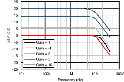
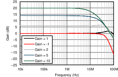
VO = 10 mVPP
Figure 1. Small-Signal Frequency Response for Various Gains
OPA2626 C006_SBOS688.png
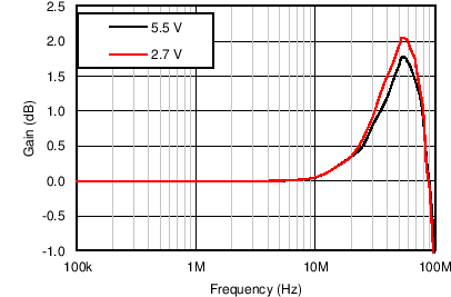
VO = 10 mVPP, G = 1
Figure 3. Small-Signal Frequency Response for Various Power Supply Voltages
OPA2626 C008_SBOS688.png
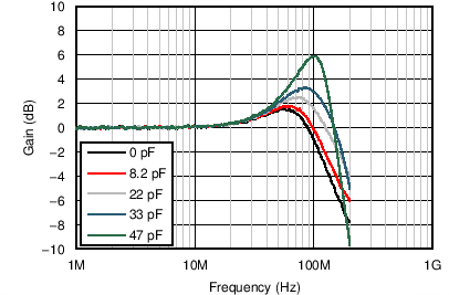
VO = 2 VPP, G = 1
Figure 5. Large-Signal Frequency Response for Various Capacitive Loads
OPA2626 C024_SBOS688.png
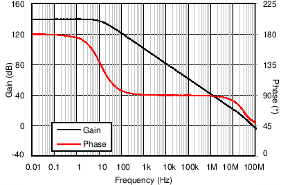
VO = 10 mVPP
Figure 7. Open-Loop Gain and Phase vs Frequency
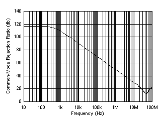
OPA2626 D007_SBOS690.gif
Figure 9. Common-Mode Rejection Ratio vs Frequency
OPA2626 C023_SBOS688.png
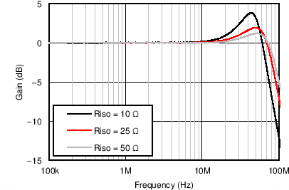
G = 1, CLOAD = 1.2 nF
Figure 11. Series Resistance for Capacitive Load Stability
OPA2626 C028_SBOS688.png
G = –1, VO = 10 mVPP
Figure 13. Overshoot vs Capacitive Load, G = –1
OPA2626 C011_SBOS688.png
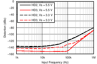
G = 1, VO = 2 VPP, RLOAD = 600 Ω
Figure 15. Distortion vs Frequency for Various Power Supplies
OPA2626 C013_SBOS688.png
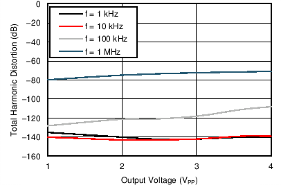
G = 1, RLOAD = 600 Ω
Figure 17. Total Harmonic Distortion vs Output Voltage for Various Frequencies
OPA2626 C015_SBOS688.png
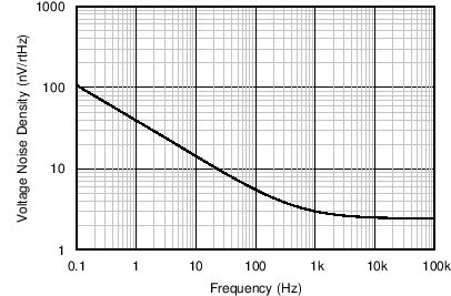
Figure 19. Voltage Noise Density vs Frequency
OPA2626 D200_sbos688.gif
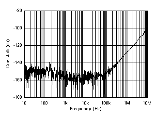
Figure 21. Crosstalk vs Frequency
OPA2626 C018_SBOS688.png
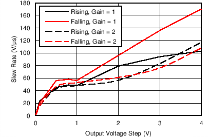
Figure 23. Slew Rate vs Output Step Size
OPA2626 C020_SBOS688.png
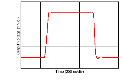
G = 1, VO = 4-V step
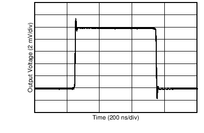
Figure 25. Large-Signal Pulse Response
OPA2626 C029_SBOS688.png
G = 1, VO = 10-mV step
Figure 27. Small-Signal Pulse Response
OPA2626 C034_SBOS688.png
VO = 3.6-V step at t = 0 s
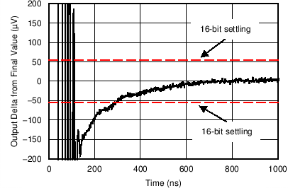
Figure 29. 16-Bit Negative Settling Time
OPA2626 C031_SBOS688.png
VS = ±2.75 V, G = 1
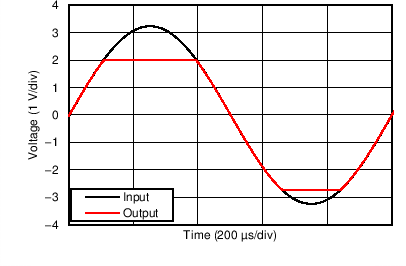
Figure 31. No Phase Reversal
OPA2626 C022_SBOS688.png
VS = ±2.75 V, G = 5
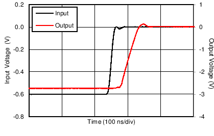
Figure 33. Negative Overload Recovery
OPA2626 C014_OT.png
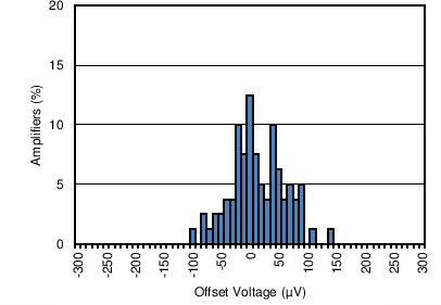
Distribution taken from 80 amplifiers, TA = 125°C
Figure 35. Input Offset Voltage Distribution
OPA2626 C006_OT.png
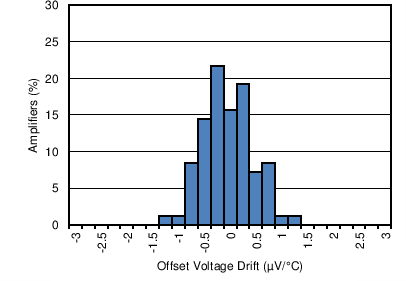
Distribution taken from 75 amplifiers, TA = –40°C to +125°C
Figure 37. Input Offset Voltage Drift Distribution
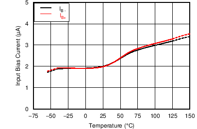
OPA2626 C020_OT.png
Figure 39. Input Bias Current vs Temperature
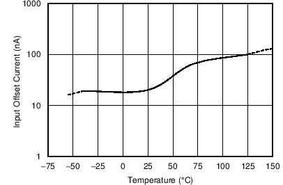
OPA2626 C021_OT.png
Figure 41. Input Offset Current vs Temperature
OPA2626 C010_OT.png
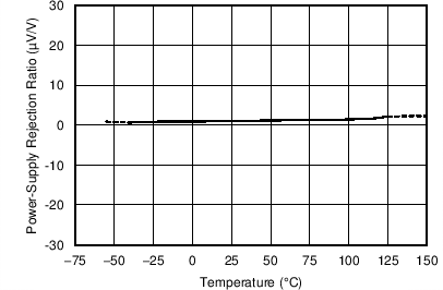
2.7 V ≤ VS ≤ 5.5 V
Figure 43. Power-Supply Rejection Ratio vs Temperature
OPA2626 C013_OT.png
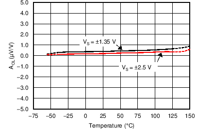
RLOAD = 600 Ω
Figure 45. Open-Loop Gain vs Temperature With 600-Ω Load
OPA2626 C009_OT.png
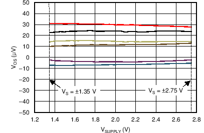
6 typical units shown, VS = ±1.35 V to ±2.75 V
Figure 47. Input Offset Voltage vs Power-Supply Voltage
OPA2626 C004_OT.png
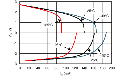
Figure 49. Output Voltage vs Output Current
OPA2626 C001_OT.png
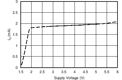
Figure 51. Quiescent Current vs Power-Supply Voltage
OPA2626 D006_SBOS688.gif
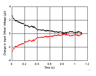
Powered on at t = 0 s, PCB dimensions: 4 in2, 2 layer, FR4
Figure 53. Warm-Up Time
OPA2626 C005_SBOS688.png
VO = 2 VPP
Figure 2. Large-Signal Frequency Response for Various Gains
OPA2626 C007_SBOS688.png
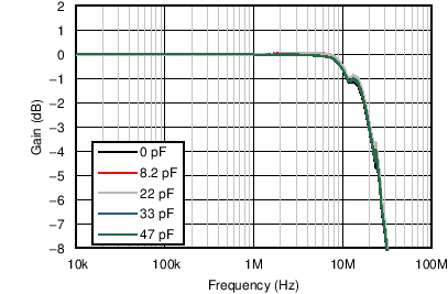
VO = 10 mVPP , G = 1
Figure 4. Small-Signal Frequency Response for Various Capacitive Loads
OPA2626 C009_SBOS688.png
VO = 10 mVPP , G = 1
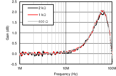
Figure 6. Small-Signal Frequency Response for Various Resistive Loads
OPA2626 D003_SBOS688.gif
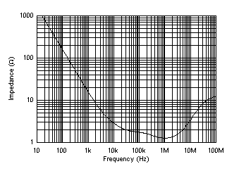
Figure 8. Open-Loop Output Impedance vs Frequency
OPA2626 C026_SBOS688.png
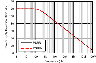
Figure 10. Power-Supply Rejection Ratio vs Frequency
OPA2626 C027_SBOS688.png
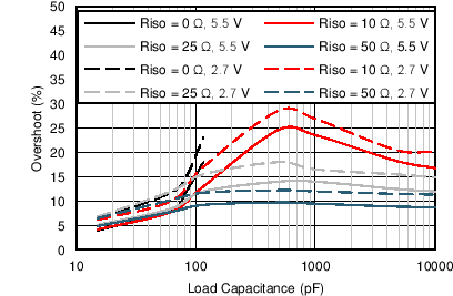
G = 1, VO = 10 mVPP
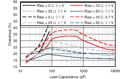
Figure 12. Overshoot vs Capacitive Load, G = 1
OPA2626 C010_SBOS688.png
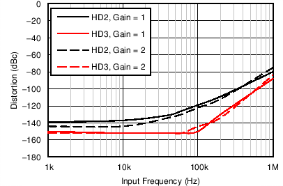
VS = 5.5 V, VO = 2 VPP, RLOAD = 600 Ω
Figure 14. Distortion vs Frequency for Various Gains
OPA2626 C012_SBOS688.png
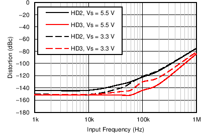
G = 2, VO = 2 VPP, RLOAD = 600 Ω
Figure 16. Distortion vs Frequency for Various Power Supplies
OPA2626 C014_SBOS688.png
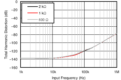
G = 1, VO = 2 VPP , RLOAD = 600 Ω
Figure 18. Total Harmonic Distortion vs Frequency for Various Loads
OPA2626 C016_SBOS688.png
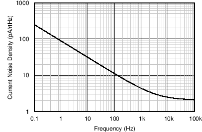
Figure 20. Current Noise Density vs Frequency
OPA2626 C017_SBOS688.png
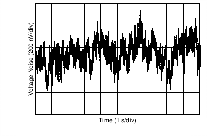
Figure 22. 0.1-Hz to 10-Hz Voltage Noise
OPA2626 D001_SBOS688.gif
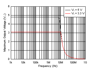
Figure 24. Maximum Output Voltage vs Frequency
OPA2626 C019_SBOS688.png
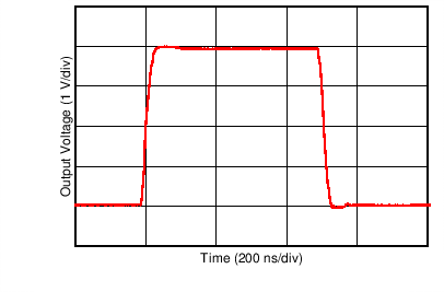
G = –1, VO = 4-V step
Figure 26. Large-Signal Pulse Response
OPA2626 C030_SBOS688.png
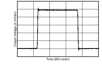
G = –1, VO = 10-mV step
Figure 28. Small-Signal Pulse Response
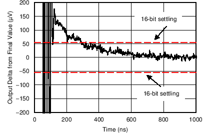
OPA2626 C033_SBOS688.png
VO = 3.6-V step at t = 0 s
Figure 30. 16-Bit Positive Settling Time
OPA2626 C021_SBOS688.png
VS = ±2.75 V, G = 5
Figure 32. Positive Overload Recovery
OPA2626 C007_OT.png
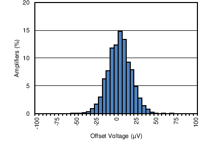
Distribution taken from 3139 amplifiers, TA = 25°C
Figure 34. Input Offset Voltage Distribution
OPA2626 C016_OT.png
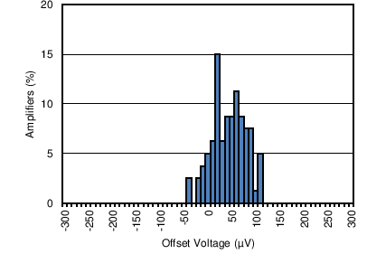
Distribution taken from 80 amplifiers, TA = –40°C
Figure 36. Input Offset Voltage Distribution
OPA2626 C022_OT.png
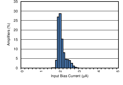
Distribution taken from 3139 amplifiers
Figure 38. Input Bias Current Distribution
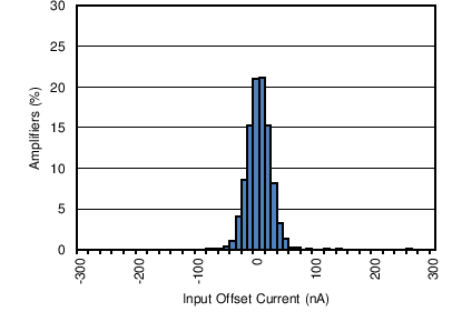
OPA2626 C023_OT.png
Distribution taken from 3139 amplifiers
Figure 40. Input Offset Current Distribution
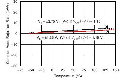
OPA2626 C011_OT.png
Figure 42. Common-Mode Rejection Ratio vs Temperature
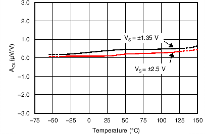
OPA2626 C012_OT.png
RLOAD = 10 kΩ
Figure 44. Open-Loop Gain vs Temperature With 10-kΩ Load
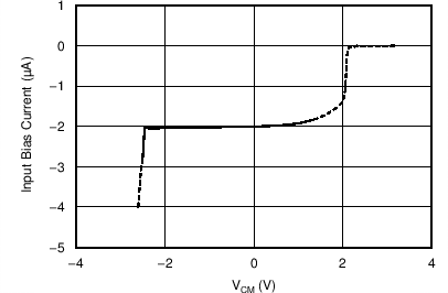
OPA2626 C019_OT.png
VS = ±2.5 V
Figure 46. Input Bias Current vs Input Common-Mode Voltage
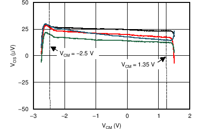
OPA2626 C008_OT.png
6 typical units shown, VS = ±2.5 V
Figure 48. Input Offset Voltage vs Common-Mode Voltage
OPA2626 C003OT.png
Figure 50. Short-Circuit Current vs Temperature
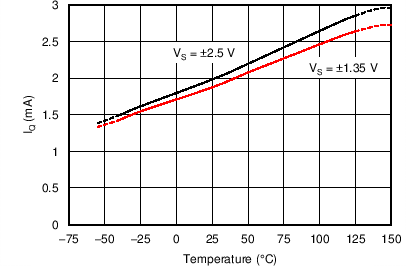
OPA2626 C017_OT.png
Figure 52. Quiescent Current vs Temperature