ZHCSF85A July   2016  – December 2019 OPA2626

PRODUCTION DATA.  

  1. 特性
  2. 应用
  3. 说明
    1.     Device Images
      1.      SAR ADC 驱动器
      2.      高保真拓扑改善了动态性能 (fIN = 10kHz,1MSPS FFT)
  4. 修订历史记录
  5. Pin Configuration and Functions
    1.     Pin Functions: OPA2626
  6. Specifications
    1. 6.1 Absolute Maximum Ratings
    2. 6.2 ESD Ratings
    3. 6.3 Recommended Operating Conditions
    4. 6.4 Thermal Information
    5. 6.5 Electrical Characteristics: High-Supply
    6. 6.6 Electrical Characteristics: Low-Supply
    7. 6.7 Typical Characteristics
  7. Parameter Measurement Information
    1. 7.1 DC Parameter Measurements
    2. 7.2 Transient Parameter Measurements
    3. 7.3 AC Parameter Measurements
    4. 7.4 Noise Parameter Measurements
  8. Detailed Description
    1. 8.1 Overview
    2. 8.2 Functional Block Diagram
    3. 8.3 Feature Description
      1. 8.3.1 SAR ADC Driver
      2. 8.3.2 Electrical Overstress
    4. 8.4 Device Functional Modes
      1. 8.4.1 High-Drive Mode
  9. Application and Implementation
    1. 9.1 Application Information
    2. 9.2 Typical Applications
      1. 9.2.1 Single-Supply, 16-Bit, 1-MSPS SAR ADC Driver
        1. 9.2.1.1 Design Requirements
        2. 9.2.1.2 Detailed Design Procedure
        3. 9.2.1.3 Application Curve
      2. 9.2.2 Single-Supply, 16-Bit, 1-MSPS, Multiplexed, SAR ADC Driver
        1. 9.2.2.1 Design Requirements
        2. 9.2.2.2 Detailed Design Procedure
        3. 9.2.2.3 Application Curves
  10. 10Power Supply Recommendations
  11. 11Layout
    1. 11.1 Layout Guidelines
    2. 11.2 Layout Example
  12. 12器件和文档支持
    1. 12.1 器件支持
      1. 12.1.1 开发支持
        1. 12.1.1.1 TINA-TI(免费软件下载)
        2. 12.1.1.2 TI 高精度设计
    2. 12.2 文档支持
      1. 12.2.1 相关文档
    3. 12.3 接收文档更新通知
    4. 12.4 社区资源
    5. 12.5 商标
    6. 12.6 静电放电警告
    7. 12.7 Glossary
  13. 13机械、封装和可订购信息

封装选项

机械数据 (封装 | 引脚)
散热焊盘机械数据 (封装 | 引脚)
订购信息

DC Parameter Measurements

The circuit shown in Figure 54 measures the dc input offset related parameters of the OPA2626. Input offset voltage, power-supply rejection ratio, common-mode rejection ratio, and open-loop gain can be measured with this circuit. The basic test procedure requires setting the inputs (the power-supply voltage, VS, and the common-mode voltage, VCM), to the desired values. VO is set to the desired value by adjusting the loop-drive voltage while measuring VO. After all inputs are configured, measure the input offset at the VX measurement point. Calculate the input offset voltage by dividing the measured result by 101. Changing the voltages on the various inputs changes the input offset voltage. The input parameters can be measured according to the relationships illustrated in Equation 1 through Equation 5.
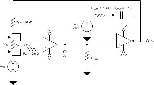
OPA2626 DC_Param_test_ckt_sbos690.gifFigure 54. DC-Parameters Measurement Circuit
Equation 1. OPA2626 q_vos_bos688.gif
Equation 2. OPA2626 q_vosdrift_bos688.gif
Equation 3. OPA2626 q_psrr_bos688.gif
Equation 4. OPA2626 q_cmrr_bos688.gif
Equation 5. OPA2626 q_aol_bos688.gif