ZHCSF85A July   2016  – December 2019 OPA2626

PRODUCTION DATA.  

  1. 特性
  2. 应用
  3. 说明
    1.     Device Images
      1.      SAR ADC 驱动器
      2.      高保真拓扑改善了动态性能 (fIN = 10kHz,1MSPS FFT)
  4. 修订历史记录
  5. Pin Configuration and Functions
    1.     Pin Functions: OPA2626
  6. Specifications
    1. 6.1 Absolute Maximum Ratings
    2. 6.2 ESD Ratings
    3. 6.3 Recommended Operating Conditions
    4. 6.4 Thermal Information
    5. 6.5 Electrical Characteristics: High-Supply
    6. 6.6 Electrical Characteristics: Low-Supply
    7. 6.7 Typical Characteristics
  7. Parameter Measurement Information
    1. 7.1 DC Parameter Measurements
    2. 7.2 Transient Parameter Measurements
    3. 7.3 AC Parameter Measurements
    4. 7.4 Noise Parameter Measurements
  8. Detailed Description
    1. 8.1 Overview
    2. 8.2 Functional Block Diagram
    3. 8.3 Feature Description
      1. 8.3.1 SAR ADC Driver
      2. 8.3.2 Electrical Overstress
    4. 8.4 Device Functional Modes
      1. 8.4.1 High-Drive Mode
  9. Application and Implementation
    1. 9.1 Application Information
    2. 9.2 Typical Applications
      1. 9.2.1 Single-Supply, 16-Bit, 1-MSPS SAR ADC Driver
        1. 9.2.1.1 Design Requirements
        2. 9.2.1.2 Detailed Design Procedure
        3. 9.2.1.3 Application Curve
      2. 9.2.2 Single-Supply, 16-Bit, 1-MSPS, Multiplexed, SAR ADC Driver
        1. 9.2.2.1 Design Requirements
        2. 9.2.2.2 Detailed Design Procedure
        3. 9.2.2.3 Application Curves
  10. 10Power Supply Recommendations
  11. 11Layout
    1. 11.1 Layout Guidelines
    2. 11.2 Layout Example
  12. 12器件和文档支持
    1. 12.1 器件支持
      1. 12.1.1 开发支持
        1. 12.1.1.1 TINA-TI(免费软件下载)
        2. 12.1.1.2 TI 高精度设计
    2. 12.2 文档支持
      1. 12.2.1 相关文档
    3. 12.3 接收文档更新通知
    4. 12.4 社区资源
    5. 12.5 商标
    6. 12.6 静电放电警告
    7. 12.7 Glossary
  13. 13机械、封装和可订购信息

封装选项

机械数据 (封装 | 引脚)
散热焊盘机械数据 (封装 | 引脚)
订购信息

Design Requirements

A SAR ADC, such as the ADS8860 device, uses sampling capacitors on the data converter input. During the signal acquisition phase, these sampling capacitors are connected to the ADC analog input terminals AINP and AINN (pins 3 and 4), through a set of switches. After the acquisition period has elapsed, the internal sampling capacitors are disconnected from the input terminals (pins 3 and 4) and connected to the ADC input through a second set of switches, during this period the ADC is performing the analog-to-digital conversion. Figure 62 shows this architecture.
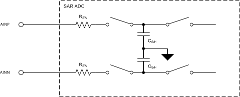
OPA2626 SAR_ADC_Simplified_Input_sbos688.gifFigure 62. Simplified SAR ADC Input

The SAR ADC inputs and sampling capacitors must be driven by the OPA2626 to 16-bit levels within the acquisition time of the ADC. For the example illustrated in Figure 61, the OPA2626 is used to drive the ADS8860 at a sample rate of 1 MSPS.