ZHCSJY2A June 2019 – September 2019 OPA2834
PRODUCTION DATA.
- 1 特性
- 2 应用
- 3 说明
- 4 修订历史记录
- 5 Device Comparison Table
- 6 Pin Configuration and Functions
- 7 Specifications
- 8 Detailed Description
- 9 Application and Implementation
- 10Power Supply Recommendations
- 11Layout
- 12器件和文档支持
- 13机械、封装和可订购信息
8.3.3 Low-Power Applications and the Effects of Resistor Values on Bandwidth
Choosing the right value of feedback resistor (RF) gives the lowest operating current, maximum bandwidth, lowest DC error, and the best pulse response. In this section for simplicity, the main focus of the signal chain design is assumed to be the total operating current. The feedback resistor used to set the gain value invariably loads the amplifier. For example, in a gain of 2 with RF = RG = 3.6 kΩ (see Figure 48) and VOUT = 4 V (assumed), 555 µA of current flows through the feedback path to ground. However, using a 3.6-kΩ resistor may not be practical in low-power applications.
In low-power applications, there is a tendency to reduce the current consumed by the amplifier by increasing the gain-setting resistor values in the feedback path. Using larger value gain resistors has two primary side effects (other than lower power), because of the interaction of the resistors with parasitic circuit capacitance. These large-value resistors:
- Lower the bandwidth as a result of the interaction with the parasitic capacitor
- Lower the phase margin by causing
- Peaking in the frequency response
- Overshoot and ringing in the pulse response
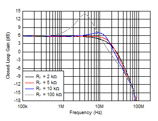
Figure 47 shows the small-signal frequency response for a noninverting gain of 2 with RF and RG equal to 2 kΩ, 5 kΩ, 10 kΩ, and 100 kΩ. The test was done with RL = 5 kΩ. Peaking reduces with lower values of RL.
 Figure 47. Frequency Response With Various Gain-Setting Resistor Values
 As expected, larger value gain resistors result in gain peaking in the frequency response plots (peaking in the frequency response is synonymous with the reduced phase margin).
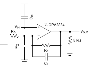
However, there is a simple way to get the best of both worlds. An ideal application requires a high value of RF for a particular gain to reduce the operating current but be limited by the reduced phase margin from the interaction of RF and CIN. The trick is simple: adding a capacitor in parallel with RF helps compensate the phase margin and restores the flat frequency response (avoids gain peaking). The value of C chosen must be such that RF × CF = CIN × RG. CIN for the OPA2834 is 1.1 pF. This value of CIN is listed in the Electrical Characteristics: 3V to 5V table as common-mode input impedance. For the case discussed here with a Gain = 2, RF = RG = 3.6 kΩ, , CIN = 1.1 pF, using a CF equal to 1 pF is sufficient to reduce the gain peaking. Using a CF equal to 1 pF enables users to increase the values of RF and RG to much higher values beyond 3.6 kΩ to reduce the operational current consumed by the amplifier.
Figure 48 shows the test circuit.
 Figure 48. G = 2 Test Circuit for Various Gain-Setting Resistor Values