ZHCSJY2A June 2019 – September 2019 OPA2834
PRODUCTION DATA.
- 1 特性
- 2 应用
- 3 说明
- 4 修订历史记录
- 5 Device Comparison Table
- 6 Pin Configuration and Functions
- 7 Specifications
- 8 Detailed Description
- 9 Application and Implementation
- 10Power Supply Recommendations
- 11Layout
- 12器件和文档支持
- 13机械、封装和可订购信息
8.4.2 Single-Supply Operation (2.7 V to 5.4 V)
Often, newer systems use a single power supply to improve efficiency and reduce the cost of the power supply. The OPA2834 is designed for use with single-supply power operation and can be used with single-supply power with no change in performance from split supply, as long as the input and output are biased within the linear operation of the device.
To change the circuit from split-supply to single-supply, level shift all voltages by half the difference between the power-supply rails. For example, Figure 51 shows changing from a ±2.5-V split supply to a 5-V single supply.
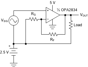 Figure 51. Single-Supply Concept
 A practical circuit has an amplifier or some other circuit providing the bias voltage for the input, and the output of this amplifier stage provides the bias for the next stage.
Figure 52 shows a typical noninverting amplifier circuit. With a 5-V single-supply, a mid-supply reference generator is needed to bias the negative side through RG. To cancel the voltage offset that is otherwise caused by the input bias currents, R1 is selected to be equal to RF in parallel with RG. For example, if a gain of 2 is required and RF = 3.6 kΩ, select RG = 3.6 kΩ to set the gain, and R1 = 1.8 kΩ for bias current cancellation. The value for C is dependent on the reference, and TI recommends a value of at least 0.1 µF to limit noise.
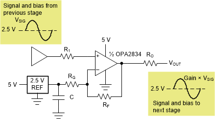 Figure 52. Noninverting Single-Supply Operation With Reference
 Figure 53 illustrates a similar noninverting single-supply scenario with the reference generator replaced by the Thevenin equivalent using resistors and the positive supply. RG’ and RG” form a resistor divider from the 5-V supply and are used to bias the negative side with the parallel sum equal to the equivalent RG to set the gain. To cancel the voltage offset that is otherwise caused by the input bias currents, R1 is selected to be equal to RF in parallel with RG’ in parallel with RG” (R1= RF || RG’ || RG”). For example, if a gain of 2 is required and RF = 3.6 kΩ, selecting RG’ = RG” = 7.2 kΩ gives an equivalent parallel sum of 3.6 kΩ, sets the gain to 2, and references the input to mid supply (2.5 V). R1 is set to 1.8 kΩ for bias current cancellation. The resistor divider costs less than the 2.5-V reference in Figure 53 but can increase the current from the 5-V supply.
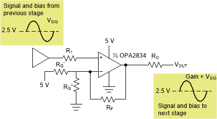 Figure 53. Noninverting Single-Supply Operation With Resistors
 Figure 54 shows a typical inverting-amplifier circuit. With a 5-V single-supply, a mid-supply reference generator is needed to bias the positive side through R1. To cancel the voltage offset that is otherwise caused by the input bias currents, R1 is selected to be equal to RF in parallel with RG. For example, if a gain of –2 is required and RF = 3.6 kΩ, select RG = 1.8 kΩ to set the gain and R1 = 1.2 kΩ for bias current cancellation. The value for C is dependent on the reference, but TI recommends a value of at least 0.1 µF to limit noise into the op amp.
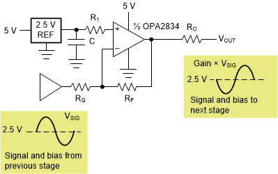 Figure 54. Inverting Single-Supply Operation With Reference
 Figure 55 illustrates a similar inverting single-supply scenario with the reference generator replaced by the Thevenin equivalent using resistors and the positive supply. R1 and R2 form a resistor divider from the 5-V supply and are used to bias the positive side. To cancel the voltage offset that is otherwise caused by the input bias currents, set the parallel sum of R1 and R2 equal to the parallel sum of RF and RG. C must be added to limit the coupling of noise into the positive input. For example, if a gain of –2 is required and RF = 3.6 kΩ, select RG = 1.8 kΩ to set the gain. R1 = R2 = 2.4 kΩ for the mid-supply voltage bias and for op-amp input-bias current cancellation. A good value for C is 0.1 µF. The resistor divider costs less than the 2.5-V reference in Figure 55 but can increase the current from the 5-V supply.
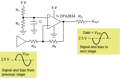 Figure 55. Inverting Single-Supply Operation With Resistors