ZHCS020J January 2011 – March 2021 OPA2835 , OPA835
PRODUCTION DATA
- 1 特性
- 2 应用
- 3 说明
- 4 Revision History
- 5 Device Comparision Table
- 6 Pin Configuration and Functions
-
7 Specifications
- 7.1 Absolute Maximum Ratings
- 7.2 ESD Ratings
- 7.3 Recommended Operating Conditions
- 7.4 Thermal Information: OPA835
- 7.5 Thermal Information: OPA2835
- 7.6 Electrical Characteristics: VS = 2.7 V
- 7.7 Electrical Characteristics: VS = 5 V
- 7.8 Typical Characteristics: VS = 2.7 V
- 7.9 Typical Characteristics: VS = 5 V
- 8 Detailed Description
-
9 Application and Implementation
- 9.1
Application Information
- 9.1.1 Noninverting Amplifier
- 9.1.2 Inverting Amplifier
- 9.1.3 Instrumentation Amplifier
- 9.1.4 Attenuators
- 9.1.5 Single-Ended to Differential Amplifier
- 9.1.6 Differential to Single-Ended Amplifier
- 9.1.7 Differential-to-Differential Amplifier
- 9.1.8 Gain Setting With OPA835 RUN Integrated Resistors
- 9.1.9 Pulse Application With Single-Supply
- 9.1.10 ADC Driver Performance
- 9.2 Typical Application
- 9.1
Application Information
- 10Power Supply Recommendations
- 11Layout
- 12Device and Documentation Support
- 13Mechanical, Packaging, and Orderable Information
封装选项
机械数据 (封装 | 引脚)
散热焊盘机械数据 (封装 | 引脚)
订购信息
6 Pin Configuration and Functions
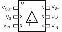 Figure 6-1 OPA835: DBV Package6-Pin SOT-23Top View
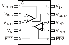 Figure 6-3 OPA2835: DGS Package10-Pin VSSOPTop View
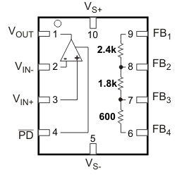 Figure 6-5 OPA835: RUN Package10-Pin QFNTop View
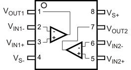 Figure 6-2 OPA2835: D Package8-Pin SOICTop View
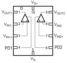 Figure 6-4 OPA2835: RMC and RUN Packages10-Pin UQFN and 10-Pin QFNTop View
Table 6-1 Pin Functions
| PIN | I/O | DESCRIPTION | |||||
|---|---|---|---|---|---|---|---|
| NAME | OPA835 | OPA2835 | |||||
| SOT-23 | QFN | SOIC | VSSOP | QFN, UQFN |
|||
| FB1 | — | 9 | — | — | — | I/O | Connection to top of 2.4-kΩ internal gain-setting resistors |
| FB2 | 8 | I/O | Connection to junction of 1.8-kΩ and 2.4-kΩ internal gain-setting resistors | ||||
| FB3 | 7 | I/O | Connection to junction of 600-Ω and 1.8-kΩ internal gain-setting resistors | ||||
| FB4 | 6 | I/O | Connection to bottom of 600-Ω internal gain-setting resistors | ||||
| PD | 5 | 4 | I | Amplifier Power Down, low = low-power mode, high = normal operation (PIN MUST BE DRIVEN) |
|||
| PD1 | — | — | 5 | 4 | I | Amplifier 1 Power Down, low = low-power mode, high = normal operation (PIN MUST BE DRIVEN) |
|
| PD2 | 6 | 6 | I | Amplifier 2 Power Down, low = low-power mode, high = normal operation (PIN MUST BE DRIVEN) |
|||
| VIN+ | 3 | 3 | — | — | I | Amplifier noninverting input | |
| VIN– | 4 | 2 | I | Amplifier inverting input | |||
| VIN1+ | — | — | 3 | 3 | 3 | I | Amplifier 1 noninverting input |
| VIN1– | 2 | 2 | 2 | I | Amplifier 1 inverting input | ||
| VIN2+ | 5 | 7 | 7 | I | Amplifier 2 noninverting input | ||
| VIN2– | 6 | 8 | 8 | I | Amplifier 2 inverting input | ||
| VOUT | 1 | 1 | — | — | — | O | Amplifier output |
| VOUT1 | — | — | 1 | 1 | 1 | O | Amplifier 1 output |
| VOUT2 | 7 | 9 | 9 | O | Amplifier 2 output | ||
| VS+ | 6 | 10 | 8 | 10 | 10 | POW | Positive power supply input |
| VS– | 2 | 5 | 4 | 4 | 5 | POW | Negative power supply input |