ZHCSFQ4 December 2016 OPA2836-Q1
PRODUCTION DATA.
- 1 特性
- 2 应用
- 3 说明
- 4 修订历史记录
- 5 OPA2836-Q1 Related Devices
- 6 Pin Configuration and Functions
- 7 Specifications
- 8 Detailed Description
-
9 Application and Implementation
- 9.1
Application Information
- 9.1.1 Noninverting Amplifier
- 9.1.2 Inverting Amplifier
- 9.1.3 Instrumentation Amplifier
- 9.1.4 Attenuators
- 9.1.5 Single-Ended-to-Differential Amplifier
- 9.1.6 Differential-to-Signal-Ended Amplifier
- 9.1.7 Differential-to-Differential Amplifier
- 9.1.8 Pulse Application With Single-Supply
- 9.1.9 ADC Driver Performance
- 9.2 Typical Applications
- 9.1
Application Information
- 10Power Supply Recommendations
- 11Layout
- 12器件和文档支持
- 13机械、封装和可订购信息
7 Specifications
7.1 Absolute Maximum Ratings
over operating free-air temperature range (unless otherwise noted)(1)| MIN | MAX | UNIT | |||
|---|---|---|---|---|---|
| VS– to VS+ | Supply voltage | 5.5 | V | ||
| VI | Input voltage | VS– – 0.7 | VS+ + 0.7 | V | |
| VID | Differential input voltage | 1 | V | ||
| II | Continuous input current | 0.85 | mA | ||
| IO | Continuous output current | 60 | mA | ||
| Continuous power dissipation | See Thermal Information | ||||
| TJ | Maximum junction temperature | 150 | °C | ||
| TA | Operating free-air temperature | –40 | 125 | °C | |
| Tstg | Storage temperature | –65 | 150 | °C | |
(1) Stresses beyond those listed under Absolute Maximum Ratings may cause permanent damage to the device. These are stress ratings only, which do not imply functional operation of the device at these or any other conditions beyond those indicated under Recommended Operating Conditions. Exposure to absolute-maximum-rated conditions for extended periods may affect device reliability.
7.2 ESD Ratings
| VALUE | UNIT | |||
|---|---|---|---|---|
| V(ESD) | Electrostatic discharge | Human body model (HBM), per AEC Q100-002(1) | ±6000 | V |
| Charged-device model (CDM), per AEC Q100-011 | ±1000 | |||
(1) AEC Q100-002 indicates that HBM stressing shall be in accordance with the ANSI/ESDA/JEDEC JS-001 specification.
7.3 Recommended Operating Conditions
over operating free-air temperature range (unless otherwise noted)| MIN | NOM | MAX | UNIT | ||
|---|---|---|---|---|---|
| VS+ | Single supply voltage | 2.5 | 5 | 5.5 | V |
| TA | Ambient temperature | –40 | 25 | 125 | °C |
7.4 Thermal Information
| THERMAL METRIC(1) | OPA2836-Q1 | UNIT | |
|---|---|---|---|
| DGK (VSSOP) | |||
| 8 PINS | |||
| RθJA | Junction-to-ambient thermal resistance | 177.7 | °C/W |
| RθJCtop | Junction-to-case (top) thermal resistance | 69.3 | °C/W |
| RθJB | Junction-to-board thermal resistance | 98.8 | °C/W |
| ψJT | Junction-to-top characterization parameter | 11.7 | °C/W |
| ψJB | Junction-to-board characterization parameter | 97.2 | °C/W |
(1) For more information about traditional and new thermal metrics, see the Semiconductor and IC Package Thermal Metrics application report.
7.5 Electrical Characteristics: VS = 2.7 V
test conditions unless otherwise noted: VS+ = 2.7 V, VS– = 0 V, VOUT = 1 VPP, RF = 0 Ω, RL = 2 kΩ, G = 1 V/V, input and output referenced to mid-supply, VIN_CM = mid-supply – 0.5 V; TA = 25°C (unless otherwise noted)| PARAMETER | TEST CONDITIONS | MIN | TYP | MAX | UNIT | TEST LEVEL(1) |
|---|---|---|---|---|---|---|
| AC PERFORMANCE | ||||||
| Small-signal bandwidth | VOUT = 100 mVPP, G = 1 | 200 | MHz | C | ||
| VOUT = 100 mVPP, G = 2 | 100 | C | ||||
| VOUT = 100 mVPP, G = 5 | 26 | C | ||||
| VOUT = 100 mVPP, G = 10 | 11 | C | ||||
| Gain-bandwidth product | VOUT = 100 mVPP, G = 10 | 110 | MHz | C | ||
| Large-signal bandwidth | VOUT = 1 VPP, G = 2 | 60 | MHz | C | ||
| Bandwidth for 0.1-dB flatness | VOUT = 1 VPP, G = 2 | 25 | MHz | C | ||
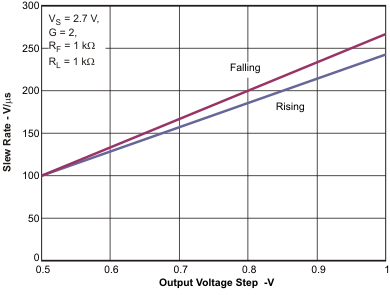
| Slew rate, rise | VOUT = 1 VSTEP, G = 2 | 260 | V/µs | C | ||
| Slew rate, fall | VOUT = 1 VSTEP, G = 2 | 240 | V/µs | C | ||
| Rise time | VOUT = 1 VSTEP, G = 2 | 4 | ns | C | ||
| Fall time | VOUT = 1 VSTEP, G = 2 | 4.5 | ns | C | ||
| Settling time to 1%, rise | VOUT = 1 VSTEP, G = 2 | 15 | ns | C | ||
| Settling time to 1%, fall | VOUT = 1 VSTEP, G = 2 | 15 | ns | C | ||
| Settling time to 0.1%, rise | VOUT = 1 VSTEP, G = 2 | 30 | ns | C | ||
| Settling time to 0.1%, fall | VOUT = 1 VSTEP, G = 2 | 25 | ns | C | ||
| Settling time to 0.01%, rise | VOUT = 1 VSTEP, G = 2 | 50 | ns | C | ||
| Settling time to 0.01%, fall | VOUT = 1 VSTEP, G = 2 | 45 | ns | C | ||
| Overshoot | VOUT = 1 VSTEP, G = 2 | 5% | C | |||
| Undershoot | VOUT = 1 VSTEP, G = 2 | 3% | C | |||
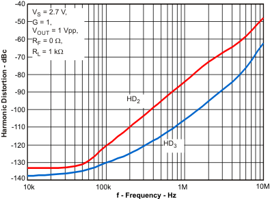
| Second-order harmonic distortion | f = 10 kHz, VIN_CM = mid-supply – 0.5 V | –133 | dBc | C | ||
| f = 100 kHz, VIN_CM = mid-supply – 0.5 V | –120 | C | ||||
| f = 1 MHz, VIN_CM = mid-supply – 0.5 V | –84 | C | ||||
| Third-order harmonic distortion | f = 10 kHz, VIN_CM = mid-supply – 0.5 V | –137 | dBc | C | ||
| f = 100 kHz, VIN_CM = mid-supply – 0.5 V | –130 | C | ||||
| f = 1 MHz, VIN_CM = mid-supply – 0.5 V | –105 | C | ||||
| Second-order intermodulation distortion | f = 1 MHz, 200-kHz tone spacing, VOUT envelope = 1 VPP, VIN_CM = mid-supply – 0.5 V |
–90 | dBc | C | ||
| Third-order intermodulation distortion | f = 1 MHz, 200-kHz tone spacing, VOUT envelope = 1 VPP, VIN_CM = mid-supply – 0.5 V |
–90 | dBc | C | ||
| Input voltage noise | f = 100 kHz | 4.6 | nV/√Hz | C | ||
| Voltage noise 1/f corner frequency | 215 | Hz | C | |||
| Input current noise | f = 1 MHz | 0.75 | pA/√Hz | C | ||
| Current noise 1/f corner frequency | 31.7 | kHz | C | |||
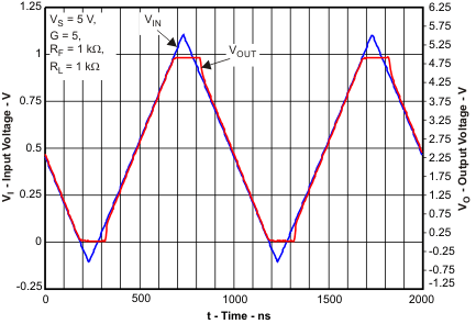
| Overdrive recovery time | Overdrive = 0.5 V | 55 | ns | C | ||
| Underdrive recovery time | Underdrive = 0.5 V | 60 | ns | C | ||
| Closed-loop output impedance | f = 100 kHz | 0.02 | Ω | C | ||
| Channel-to-channel crosstalk | f = 10 kHz | –120 | dB | C | ||
| DC PERFORMANCE | ||||||
| Open-loop voltage gain (AOL) | 100 | 125 | dB | A | ||
| Input-referred offset voltage | TA = 25°C | –400 | ±65 | 400 | µV | A |
| TA = –40°C to +85°C | –760 | 760 | B | |||
| TA = –40°C to +125°C | –1060 | 1060 | B | |||
| Input offset voltage drift(2) | TA = –40°C to +85°C | –6 | ±1 | 6 | µV/°C | B |
| TA = –40°C to +125°C | –6.6 | ±1.1 | 6.6 | B | ||
| DC PERFORMANCE (continued) | ||||||
| Input bias current(3) | TA = 25°C | 200 | 650 | 1000 | nA | A |
| TA = –40°C to +85°C | 120 | 1500 | B | |||
| TA = –40°C to +125°C | 100 | 1800 | B | |||
| Input bias current drift(2) | TA = –40°C to +85°C | –1.9 | ±0.32 | 1.9 | nA/°C | B |
| TA = –40°C to +125°C | –3.5 | ±0.37 | 2.1 | B | ||
| Input offset current | TA = 25°C | –180 | ±30 | 180 | nA | A |
| B | ||||||
| TA = –40°C to +85°C | –215 | ±30 | 215 | |||
| TA = –40°C to +125°C | –240 | ±30 | 240 | B | ||
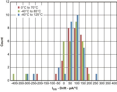
| Input offset current drift(2) | TA = –40°C to +85°C | –575 | ±95 | 575 | pA/°C | B |
| TA = –40°C to +125°C | –600 | ±100 | 600 | B | ||
| INPUT | ||||||
| Common-mode input range, low | TA = 25°C, < 3-dB degradation in CMRR limit |
–0.2 | 0 | V | A | |
| TA = –40°C to 125°C, < 3-dB degradation in CMRR limit |
–0.2 | 0 | V | B | ||
| Common-mode input range, high | TA = 25°C, < 3-dB degradation in CMRR limit |
1.5 | 1.6 | V | A | |
| TA = –40°C to 125°C, < 3-dB degradation in CMRR limit |
1.5 | 1.6 | V | B | ||
| Input linear operating voltage range | TA = 25°C, < 6-dB degradation in THD |
–0.3 to 1.75 | V | C | ||
| Common-mode rejection ratio | 91 | 114 | dB | A | ||
| Input impedance common-mode | 200 || 1.2 | kΩ || pF | C | |||
| Input impedance differential mode | 200 || 1 | kΩ || pF | C | |||
| OUTPUT | ||||||
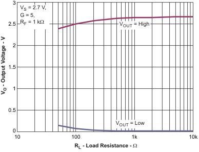
| Output voltage, low | TA = 25°C, G = 5 | 0.15 | 0.2 | V | A | |
| TA = –40°C to +125°C, G = 5 | 0.15 | 0.2 | V | B | ||
| Output voltage, high | TA = 25°C, G = 5 | 2.45 | 2.5 | V | A | |
| TA = –40°C to +125°C, G = 5 | 2.45 | 2.5 | V | B | ||
| Output saturation voltage, high | TA = 25°C, G = 5 | 80 | mV | C | ||
| Output saturation voltage, low | TA = 25°C, G = 5 | 40 | mV | C | ||
| Output current drive | TA = 25°C | ±40 | ±45 | mA | A | |
| TA = –40°C to +125°C | ±40 | ±45 | mA | B | ||
| POWER SUPPLY | ||||||
| Specified operating voltage | 2.5 | 5.5 | V | B | ||
| Quiescent operating current per amplifier | TA = 25°C | 0.7 | 0.95 | 1.15 | mA | A |
| TA = –40°C to +125°C | 0.6 | 1.6 | mA | B | ||
| Power-supply rejection ratio (±PSRR) | 91 | 108 | dB | A | ||
(1) Test levels (all values set by characterization and simulation): (A) 100% tested at 25°C; over temperature limits by characterization and simulation. (B) Not tested in production; limits set by characterization and simulation. (C) Typical value only for information.
(2) Input offset voltage drift, input bias current drift, and input offset current drift are average values calculated by taking data at the end points, computing the difference, and dividing by the temperature range.
(3) Current is considered positive out of the pin.
7.6 Electrical Characteristics: VS = 5 V
test conditions unless otherwise noted: VS+ = 5 V, VS– = 0 V, VOUT = 2 VPP, RF = 0 Ω, RL = 1 kΩ, G = 1 V/V, input and output referenced to mid-supply; TA = 25°C (unless otherwise noted)| PARAMETER | TEST CONDITIONS | MIN | TYP | MAX | UNIT | TEST LEVEL(1) |
|---|---|---|---|---|---|---|
| AC PERFORMANCE | ||||||
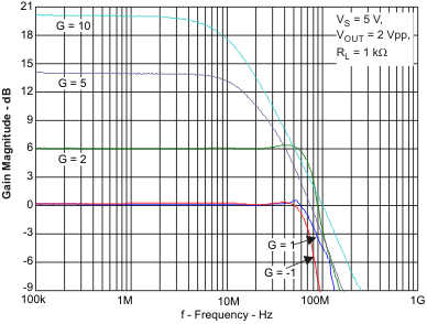
| Small-signal bandwidth | VOUT = 100 mVPP, G = 1 | 205 | MHz | C | ||
| VOUT = 100 mVPP, G = 2 | 100 | C | ||||
| VOUT = 100 mVPP, G = 5 | 28 | C | ||||
| VOUT = 100 mVPP, G = 10 | 11.8 | C | ||||
| Gain-bandwidth product | VOUT = 100 mVPP, G = 10 | 118 | MHz | C | ||
| Large-signal bandwidth | VOUT = 2 VPP, G = 2 | 87 | MHz | C | ||
| Bandwidth for 0.1-dB flatness | VOUT = 2 VPP, G = 2 | 29 | MHz | C | ||
| Slew rate, rise | VOUT = 2-V step, G = 2 | 560 | V/µs | C | ||
| Slew rate, fall | VOUT = 2-V step, G = 2 | 580 | V/µs | C | ||
| Rise time | VOUT = 2-V step, G = 2 | 3 | ns | C | ||
| Fall time | VOUT = 2-V Step, G = 2 | 3 | ns | C | ||
| Settling time to 1%, rise | VOUT = 2-V step, G = 2 | 22 | ns | C | ||
| Settling time to 1%, fall | VOUT = 2-V step, G = 2 | 22 | ns | C | ||
| Settling time to 0.1%, rise | VOUT = 2-V step, G = 2 | 30 | ns | C | ||
| Settling time to 0.1%, fall | VOUT = 2-V step, G = 2 | 30 | ns | C | ||
| Settling time to 0.01%, rise | VOUT = 2-V step, G = 2 | 40 | ns | C | ||
| Settling time to 0.01%, fall | VOUT = 2-V step, G = 2 | 45 | ns | C | ||
| Overshoot | VOUT = 2-V step, G = 2 | 7.5% | C | |||
| Undershoot | VOUT = 2-V step, G = 2 | 5% | C | |||
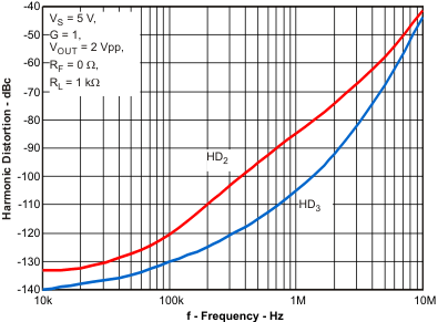
| Second-order harmonic distortion | f = 10 kHz | –133 | dBc | C | ||
| f = 100 kHz | –120 | C | ||||
| f = 1 MHz | –85 | C | ||||
| Third-order harmonic distortion | f = 10 kHz | –140 | dBc | C | ||
| f = 100 kHz | –130 | C | ||||
| f = 1 MHz | –105 | C | ||||
| Second-order intermodulation distortion | f = 1 MHz, 200-kHz tone spacing, VOUT envelope = 2 VPP |
–79 | dBc | C | ||
| Third-order intermodulation distortion | f = 1 MHz, 200-kHz tone spacing, VOUT envelope = 2 VPP |
–91 | dBc | C | ||
| Signal-to-noise ratio (SNR) | f = 1 kHz, VOUT = 1 VRMS, 22-kHz bandwidth |
0.00013% | C | |||
| –117.6 | dBc | C | ||||
| Total harmonic distortion (THD) | f = 1 kHz, VOUT = 1 VRMS | 0.00003% | C | |||
| –130 | dBc | C | ||||
| Input voltage noise | f = 100 KHz | 4.6 | nV/√Hz | C | ||
| Voltage noise 1/f corner frequency | 215 | Hz | C | |||
| Input current noise | f > 1 MHz | 0.75 | pA/√Hz | C | ||
| Current noise 1/f corner frequency | 31.7 | kHz | C | |||
| Overdrive recovery time | Overdrive = 0.5 V | 55 | ns | C | ||
| Underdrive recovery time | Underdrive = 0.5 V | 60 | ns | C | ||
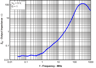
| Closed-loop output impedance | f = 100 kHz | 0.02 | Ω | C | ||
| Channel-to-channel crosstalk | f = 10 kHz | –120 | dB | C | ||
| DC PERFORMANCE | ||||||
| Open-loop voltage gain (AOL) | 100 | 122 | dB | A | ||
| Input-referred offset voltage | TA = 25°C | –400 | ±65 | 400 | µV | A |
| B | ||||||
| TA = –40°C to +85°C | –765 | 765 | ||||
| TA = –40°C to +125°C | –1080 | 1080 | B | |||
| DC PERFORMANCE (continued) | ||||||
| Input offset voltage drift(2) | TA = –40°C to +85°C | –6.1 | ±1 | 6.1 | µV/°C | B |
| TA = –40°C to +125°C | –6.8 | ±1.1 | 6.8 | B | ||
| Input bias current(3) | TA = 25°C | 200 | 650 | 1000 | nA | A |
| B | ||||||
| TA = –40°C to +85°C | 120 | 1550 | ||||
| TA = –40°C to +125°C | 100 | 1850 | B | |||
| Input bias current drift(2) | TA = –40°C to +85°C | ±0.34 | ±2 | nA/°C | B | |
| TA = –40°C to +125°C | ±0.38 | ±3.8 | B | |||
| Input offset current | TA = 25°C | ±30 | ±180 | nA | A | |
| B | ||||||
| TA = –40°C to +85°C | ±30 | ±215 | ||||
| TA = –40°C to +125°C | ±30 | ±250 | B | |||
| Input offset current drift(2) | TA = –40°C to +85°C | ±100 | ±600 | pA/°C | B | |
| TA = –40°C to +125°C | ±110 | ±660 | B | |||
| INPUT | ||||||
| Common-mode input range low | TA = 25°C, < 3-dB degradation in CMRR limit |
–0.2 | 0 | V | A | |
| TA = –40°C to 125°C, < 3-dB degradation in CMRR limit |
–0.2 | 0 | V | B | ||
| Common-mode input range high | TA = 25°C, < 3-dB degradation in CMRR limit |
3.8 | 3.9 | V | A | |
| TA = –40°C to 125°C, < 3-dB degradation in CMRR limit |
3.8 | 3.9 | V | B | ||
| Input linear operating voltage range | TA = 25°C, < 6-dB degradation in THD |
–0.3 to 4.05 | V | C | ||
| Common-mode rejection ratio | 94 | 116 | dB | A | ||
| Input impedance common mode | 200 || 1.2 | kΩ || pF | C | |||
| Input impedance differential mode | 200 || 1 | kΩ || pF | C | |||
| OUTPUT | ||||||
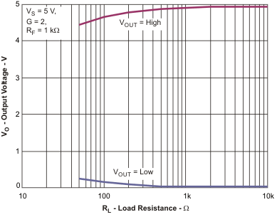
| Output voltage low | TA = 25°C, G = 5 | 0.15 | 0.2 | V | A | |
| TA = –40°C to +125°C, G = 5 | 0.15 | 0.2 | V | B | ||
| Output voltage high | TA = 25°C, G = 5 | 4.75 | 4.8 | V | A | |
| TA = –40°C to +125°C, G = 5 | 4.75 | 4.8 | V | B | ||
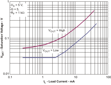
| Output saturation voltage, high | TA = 25°C, G = 5 | 100 | mV | C | ||
| Output saturation voltage, low | TA = 25°C, G = 5 | 50 | mV | C | ||
| Output current drive | TA = 25°C | ±40 | ±50 | mA | A | |
| TA = –40°C to +125°C | ±40 | ±50 | mA | B | ||
| POWER SUPPLY | ||||||
| Specified operating voltage | 2.5 | 5.5 | V | B | ||
| Quiescent operating current per amplifier | TA = 25°C | 0.8 | 1.0 | 1.2 | mA | A |
| TA = –40°C to +125°C | 0.65 | 1.7 | mA | B | ||
| Power-supply rejection ratio (±PSRR) | 94 | 108 | dB | A | ||
(1) Test levels (all values set by characterization and simulation): (A) 100% tested at 25°C; over temperature limits by characterization and simulation. (B) Not tested in production; limits set by characterization and simulation. (C) Typical value only for information.
(2) Input offset voltage drift, input bias current drift, and input offset current drift are average values calculated by taking data at the end points, computing the difference, and dividing by the temperature range.
(3) Current is considered positive out of the pin.
7.7 Typical Characteristics
7.7.1 Typical Characteristics: VS = 2.7 V
test conditions unless otherwise noted: VS+ = 2.7 V, VS– = 0 V, VOUT = 1 VPP, RF = 0 Ω, RL = 2 kΩ, G = 1 V/V, input and output referenced to mid-supply, VIN_CM = mid-supply – 0.5 V; TA = 25°C (unless otherwise noted)Table 1. Table of Graphs
| FIGURE TITLE | FIGURE LOCATION | |
|---|---|---|
| Small-Signal Frequency Response | Figure 1 | |
| Large-Signal Frequency Response | Figure 2 | |
| Noninverting Pulse Response | Figure 3 | |
| Inverting Pulse Response | Figure 4 | |
| Slew Rate vs Output Voltage Step | Figure 5 | |
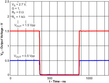
| Output Overdrive Recovery | Figure 6 | |
| Harmonic Distortion vs Frequency | Figure 7 | |
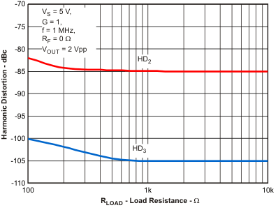
| Harmonic Distortion vs Load Resistance | Figure 8 | |
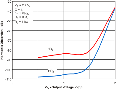
| Harmonic Distortion vs Output Voltage | Figure 9 | |
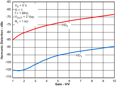
| Harmonic Distortion vs Gain | Figure 10 | |
| Output Voltage Swing vs Load Resistance | Figure 11 | |
| Output Saturation Voltage vs Load Current | Figure 12 | |
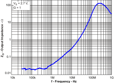
| Output Impedance vs Frequency | Figure 13 | |
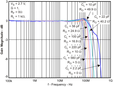
| Frequency Response With Capacitive Load | Figure 14 | |
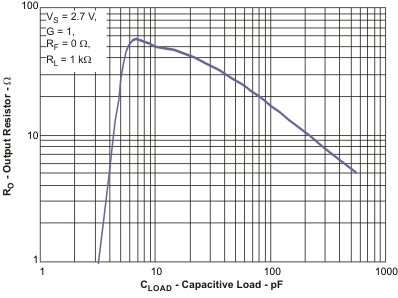
| Series Output Resistor vs Capacitive Load | Figure 17 | |
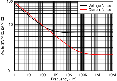
| Input-Referred Noise vs Frequency | Figure 16 | |
| Open-Loop Gain vs Frequency | Figure 15 | |
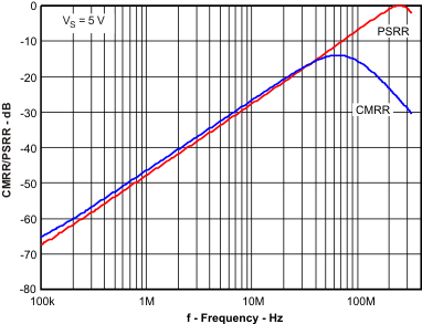
| Common-Mode, Power-Supply Rejection Ratios vs Frequency | Figure 18 | |
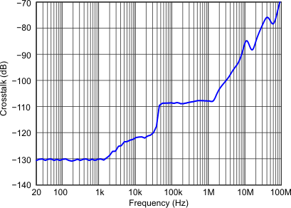
| Crosstalk vs Frequency | Figure 19 | |
| Input Offset Voltage | Figure 22 | |
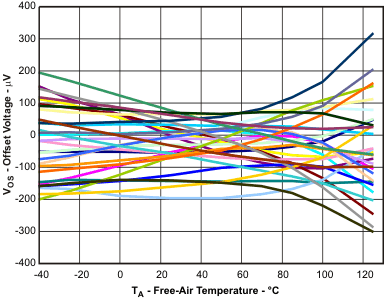
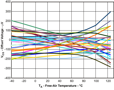
| Input Offset Voltage vs Free-Air Temperature | Figure 20 | |
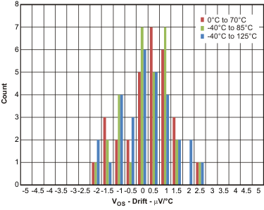
| Input Offset Voltage Drift | Figure 46 | |
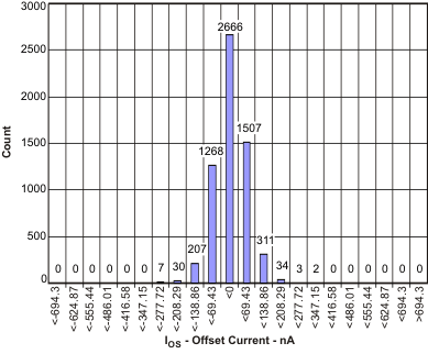
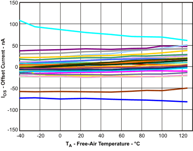
| Input Offset Current | Figure 23 | |
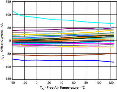
| Input Offset Current vs Free-Air Temperature | Figure 24 | |
| Input Offset Current Drift | Figure 25 | |
test conditions unless otherwise noted: VS+ = 2.7 V, VS– = 0 V, VOUT = 1 VPP, RF = 0 Ω, RL = 2 kΩ, G = 1 V/V, input and output referenced to mid-supply, VIN_CM = mid-supply – 0.5 V; TA = 25°C (unless otherwise noted)


| VS = 2.7 V |
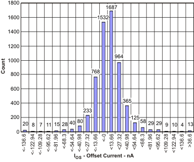
I.
Figure 23. Input Offset Current
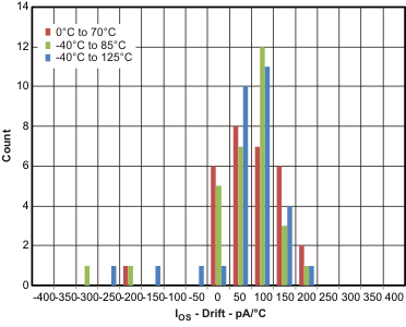
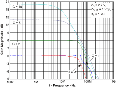
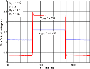
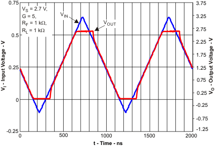
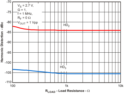
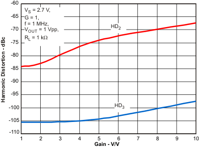
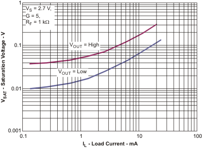
| VS = 2.7 V |

7.7.2 Typical Characteristics: VS = 5 V
test conditions unless otherwise noted: VS+ = 5 V, VS– = 0 V, VOUT = 2 VPP, RF = 0 Ω, RL = 1 kΩ, G = 1 V/V, input and output referenced to mid-supply; TA = 25°C (unless otherwise noted)Table 2. Table of Graphs
| FIGURE TITLE | FIGURE LOCATION | |
|---|---|---|
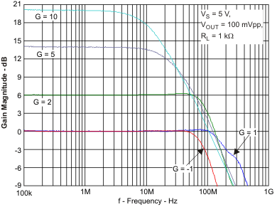
| Small-Signal Frequency Response | Figure 26 | |
| Large-Signal Frequency Response | Figure 27 | |
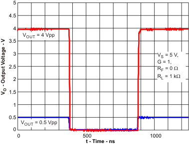
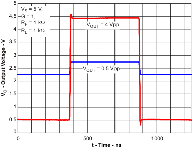
| Noninverting Pulse Response | Figure 28 | |
| Inverting Pulse Response | Figure 29 | |
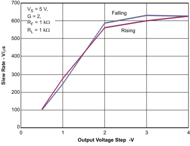
| Slew Rate vs Output Voltage Step | Figure 30 | |
| Output Overdrive Recovery | Figure 31 | |
| Harmonic Distortion vs Frequency | Figure 32 | |
| Harmonic Distortion vs Load Resistance | Figure 33 | |
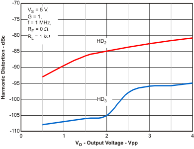
| Harmonic Distortion vs Output Voltage | Figure 34 | |
| Harmonic Distortion vs Gain | Figure 35 | |
| Output Voltage Swing vs Load Resistance | Figure 36 | |
| Output Saturation Voltage vs Load Current | Figure 37 | |
| Output Impedance vs Frequency | Figure 38 | |
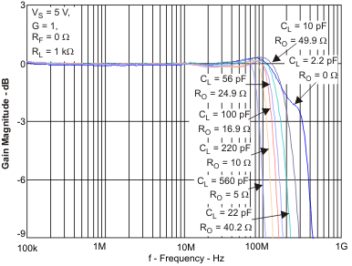
| Frequency Response With Capacitive Load | Figure 39 | |
| Series Output Resistor vs Capacitive Load | Figure 42 | |
| Input-Referred Noise vs Frequency | Figure 40 | |
| Open-Loop Gain vs Frequency | Figure 41 | |
| Common-Mode, Power-Supply Rejection Ratios vs Frequency | Figure 43 | |
| Crosstalk vs Frequency | Figure 44 | |
| Input Offset Voltage | Figure 47 | |
| Input Offset Voltage vs Free-Air Temperature | Figure 45 | |
| Input Offset Voltage Drift | Figure 46 | |
| Input Offset Current | Figure 48 | |
| Input Offset Current vs Free-Air Temperature | Figure 49 | |
| Input Offset Current Drift | Figure 50 | |
test conditions unless otherwise noted: VS+ = 5 V, VS– = 0 V, VOUT = 2 VPP, RF = 0 Ω, RL = 1 kΩ, G = 1 V/V, input and output referenced to mid-supply; TA = 25°C (unless otherwise noted)
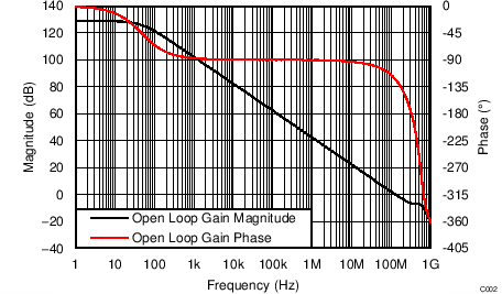
| VS = 5.0 V |
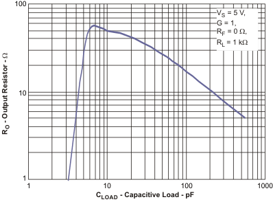

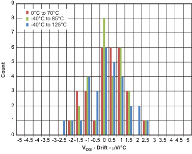
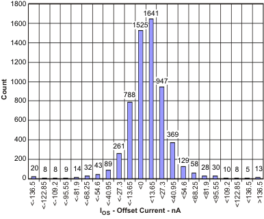

| VS = 5.0 V |
