ZHCSGP3D September 2017 – December 2018 OPA2837 , OPA837
PRODUCTION DATA.
- 1 特性
- 2 应用
- 3 说明
- 4 修订历史记录
- 5 Pin Configuration and Functions
-
6 Specifications
- 6.1 Absolute Maximum Ratings
- 6.2 ESD Ratings
- 6.3 Recommended Operating Conditions
- 6.4 Thermal Information: OPA837
- 6.5 Thermal Information: OPA2837
- 6.6 Electrical Characteristics: VS = 5 V
- 6.7 Electrical Characteristics: VS = 3 V
- 6.8 Typical Characteristics: VS = 5.0 V
- 6.9 Typical Characteristics: VS = 3.0 V
- 6.10 Typical Characteristics: ±2.5-V to ±1.5-V Split Supply
- 7 Detailed Description
-
8 Application and Implementation
- 8.1
Application Information
- 8.1.1 Noninverting Amplifier
- 8.1.2 Inverting Amplifier
- 8.1.3 Output DC Error Calculations
- 8.1.4 Output Noise Calculations
- 8.1.5 Instrumentation Amplifier
- 8.1.6 Attenuators
- 8.1.7 Differential to Single-Ended Amplifier
- 8.1.8 Differential-to-Differential Amplifier
- 8.1.9 Pulse Application With Single-Supply Circuit
- 8.1.10 ADC Driver Performance
- 8.2 Typical Applications
- 8.1
Application Information
- 9 Power Supply Recommendations
- 10Layout
- 11器件和文档支持
- 12机械、封装和可订购信息
封装选项
机械数据 (封装 | 引脚)
散热焊盘机械数据 (封装 | 引脚)
- RUN|10
订购信息
7.3.5 Low-Power Applications and the Effects of Resistor Values on Bandwidth
The OPAx837 can use a direct short in the feedback for a gain of 1 V/V. Table 2 gives a list of recommended values over gain for an increasing noninverting gain target. This table was produced by increasing the R values until they added 50% of the total output noise power. Higher values can be used to reduce power at the cost of higher noise. Lower values can be used to reduce the total output noise at the cost of more load power in the feedback network. Stability is also impaired going to very high values because of the pole introduced into the feedback path with the inverting input capacitance (1.5-pF common-mode). In low-power applications, reducing the current in the feedback path is preferable by increasing the resistor values. Using larger value resistors has two primary side effects (other than lower power) because of the interactions with the inverting input parasitic capacitance. Using large value resistors lowers the bandwidth and lowers the phase margin. When the phase margin is lowered, peaking in the frequency response and overshoot and ringing in the pulse response results.
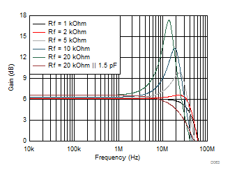
Figure 64 shows the gain = 2 V/V (6 dB) small-signal frequency response with RF and RG equal to 1 kΩ, 2 kΩ, 5 kΩ, 10 kΩ, and 20 kΩ. This test was done with RL = 2 kΩ. Lower RL values can reduce the peaking because of RL loading effects, but higher values do not have a significant effect.
 Figure 64. Frequency Response With Various RF = RG Resistor Values
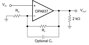
 As expected, larger value resistors cause lower bandwidth and peaking in the response (peaking in frequency response is synonymous with overshoot and ringing in pulse response). Adding a 1.5-pF capacitor in parallel with RF (equal to the input common-mode capacitance) helps compensate the phase margin loss and restores flat frequency response. Figure 65 shows the test circuit.
 Figure 65. G = 2 Test Circuit for Various Gain-Setting Resistor Values