ZHCSGP3D September 2017 – December 2018 OPA2837 , OPA837
PRODUCTION DATA.
- 1 特性
- 2 应用
- 3 说明
- 4 修订历史记录
- 5 Pin Configuration and Functions
-
6 Specifications
- 6.1 Absolute Maximum Ratings
- 6.2 ESD Ratings
- 6.3 Recommended Operating Conditions
- 6.4 Thermal Information: OPA837
- 6.5 Thermal Information: OPA2837
- 6.6 Electrical Characteristics: VS = 5 V
- 6.7 Electrical Characteristics: VS = 3 V
- 6.8 Typical Characteristics: VS = 5.0 V
- 6.9 Typical Characteristics: VS = 3.0 V
- 6.10 Typical Characteristics: ±2.5-V to ±1.5-V Split Supply
- 7 Detailed Description
-
8 Application and Implementation
- 8.1
Application Information
- 8.1.1 Noninverting Amplifier
- 8.1.2 Inverting Amplifier
- 8.1.3 Output DC Error Calculations
- 8.1.4 Output Noise Calculations
- 8.1.5 Instrumentation Amplifier
- 8.1.6 Attenuators
- 8.1.7 Differential to Single-Ended Amplifier
- 8.1.8 Differential-to-Differential Amplifier
- 8.1.9 Pulse Application With Single-Supply Circuit
- 8.1.10 ADC Driver Performance
- 8.2 Typical Applications
- 8.1
Application Information
- 9 Power Supply Recommendations
- 10Layout
- 11器件和文档支持
- 12机械、封装和可订购信息
封装选项
机械数据 (封装 | 引脚)
散热焊盘机械数据 (封装 | 引脚)
- RUN|10
订购信息
8.1.8 Differential-to-Differential Amplifier
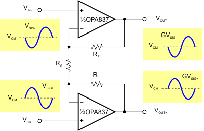
Figure 79 shows a differential amplifier that is used to amplify differential signals to a differential output. This circuit has high input impedance and is used in differential line driver applications where the signal source is a high-impedance driver (for example, a differential DAC) that must drive a line.
 Figure 79. Differential-to-Differential Amplifier
 The output of the amplifier can be calculated according to Equation 11 if VIN± is set to VCM + VSIG±.

The signal gain of the circuit is shown in Equation 12, and VCM passes with unity gain. The amplifier combines two noninverting amplifiers into one differential amplifier that shares the RG resistor, which makes RG effectively half its value when calculating the gain. The output signals are in-phase with the input signals.
