ZHCS183G May 2011 – June 2015 OPA2314 , OPA314 , OPA4314
PRODUCTION DATA.
8 Application and Implementation
NOTE
Information in the following applications sections is not part of the TI component specification, and TI does not warrant its accuracy or completeness. TI’s customers are responsible for determining suitability of components for their purposes. Customers should validate and test their design implementation to confirm system functionality.
8.1 Application Information
The OPA2314 device is a low-power, rail-to-rail input and output operational amplifier specifically designed for portable applications. The device operates from 1.8 V to 5.5 V, is unity-gain stable, and suitable for a wide range of general-purpose applications. The class AB output stage is capable of driving ≤ 10-kΩ loads connected to any point between V+ and ground. The input common-mode voltage range includes both rails, and allows the OPA2314 device to be used in virtually any single-supply application. Rail-to-rail input and output swing significantly increases dynamic range, especially in low-supply applications, and makes the device ideal for driving sampling analog-to-digital converters (ADCs).
The OPA2314 device features a 3-MHz bandwidth and 1.5-V/μs slew rate with only 150-μA supply current per channel, providing good AC performance at very low power consumption. DC applications are also well served with a very-low input noise voltage of 14 nV/√Hz at 1 kHz, low-input bias current (0.2 pA), and an input offset voltage of 0.5 mV (typical).
8.1.1 General Configurations
When receiving low-level signals, limiting the bandwidth of the incoming signals into the system is often required. The simplest way to establish this limited bandwidth is to place an RC filter at the noninverting terminal of the amplifier, as Figure 36 shows.
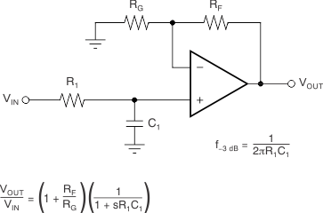 Figure 36. Single-Pole Low-Pass Filter
If even more attenuation is needed, a multiple pole filter is required. The Sallen-Key filter can be used for this task, as Figure 37 shows. For best results, the amplifier should have a bandwidth that is eight to 10 times the filter frequency bandwidth. Failure to follow this guideline can result in phase shift of the amplifier.
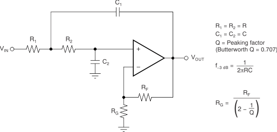 Figure 37. Two-Pole Low-Pass Sallen-Key Filter
8.1.2 Capacitive Load and Stability
The OPA2314 device is designed to be used in applications where driving a capacitive load is required. As with all op-amps, specific instances can occur where the OPA2314 device can become unstable. The particular op-amp circuit configuration, layout, gain, and output loading are some of the factors to consider when establishing whether or not an amplifier is stable in operation. An op-amp in the unity-gain (1 V/V) buffer configuration that drives a capacitive load exhibits a greater tendency to be unstable than an amplifier operated at a higher noise gain. The capacitive load, in conjunction with the op-amp output resistance, creates a pole within the feedback loop that degrades the phase margin. The degradation of the phase margin increases as the capacitive loading increases. When operating in the unity-gain configuration, the OPA2314 device remains stable with a pure capacitive load up to approximately 1 nF. The equivalent series resistance (ESR) of some very large capacitors (CL greater than 1 μF) is sufficient to alter the phase characteristics in the feedback loop such that the amplifier remains stable. Increasing the amplifier closed-loop gain allows the amplifier to drive increasingly larger capacitance. This increased capability is evident when observing the overshoot response of the amplifier at higher voltage gains. See the graph, Figure 20.
One technique for increasing the capacitive load drive capability of the amplifier operating in a unity-gain configuration is to insert a small resistor, typically 10 Ω to 20 Ω, in series with the output, as shown in Figure 38. This resistor significantly reduces the overshoot and ringing associated with large capacitive loads. One possible problem with this technique, however, is that a voltage divider is created with the added series resistor and any resistor connected in parallel with the capacitive load. The voltage divider introduces a gain error at the output that reduces the output swing.
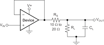 Figure 38. Improving Capacitive Load Drive
8.2 Typical Application
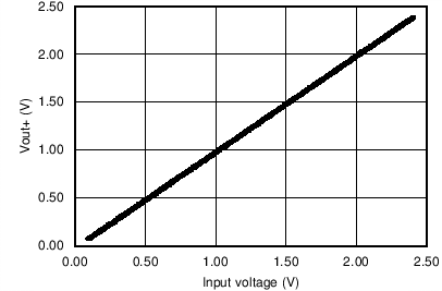
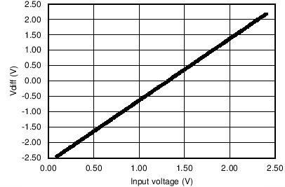
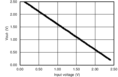
Some applications require differential signals. Figure 39 shows a simple circuit to convert a single-ended input of 0.1 V to 2.4 V into a differential output of ±2.3 V on a single 2.7-V supply. The output range is intentionally limited to maximize linearity. The circuit is composed of two amplifiers. One amplifier functions as a buffer and creates a voltage, VOUT+. The second amplifier inverts the input and adds a reference voltage to generate VOUT–. Both VOUT+ and VOUT– range from 0.1 V to 2.4 V. The difference, VDIFF, is the difference between VOUT+ and VOUT–. This makes the differential output voltage range 2.3 V.
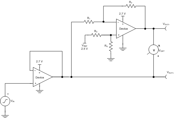 Figure 39. Schematic for a Single-Ended Input to Differential Output Conversion
8.2.1 Design Requirements
The design requirements are as follows:
- Supply voltage: 2.7 V
- Reference voltage: 2.5 V
- Input: 0.1 V to 2.4 V
- Output differential: ±2.3 V
- Output common-mode voltage: 1.25 V
- Small-signal bandwidth: 1 MHz
8.2.2 Detailed Design Procedure
The circuit in Figure 39 takes a single-ended input signal, VIN, and generates two output signals, VOUT+ and VOUT– using two amplifiers and a reference voltage, VREF. VOUT+ is the output of the first amplifier and is a buffered version of the input signal, VIN (as shown in Equation 1). VOUT– is the output of the second amplifier which uses VREF to add an offset voltage to VIN and feedback to add inverting gain. The transfer function for VOUT– is given in Equation 2.


The differential output signal, VDIFF, is the difference between the two single-ended output signals, VOUT+ and VOUT–. Equation 3 shows the transfer function for VDIFF. By applying the conditions that R1 = R2 and R3 = R4, the transfer function is simplified into Equation 6. Using this configuration, the maximum input signal is equal to the reference voltage and the maximum output of each amplifier is equal to VREF. The differential output range is 2 × VREF. Furthermore, the common-mode voltage is one half of VREF (see Equation 7).


8.2.2.1 Amplifier Selection
Linearity over the input range is key for good dc accuracy. The common-mode input range and output swing limitations determine the linearity. In general, an amplifier with rail-to-rail input and output swing is required. Bandwidth is a key concern for this design, so the OPA2314-Q1 device is selected because its bandwidth is greater than the target of 1 MHz. The bandwidth and power ratio makes this device power efficient and the low offset and drift ensure good accuracy for moderate precision applications.
8.2.2.2 Passive Component Selection
Because the transfer function of Vout– is heavily reliant on resistors (R1, R2, R3, and R4), use resistors with low tolerances to maximize performance and minimize error. This design uses resistors with resistance values of 49.9 kΩ and tolerances of 0.1%. However, if the noise of the system is a key parameter, smaller resistance values (6 kΩ or lower) can be selected to keep the overall system noise low. This ensures that the noise from the resistors is lower than the amplifier noise.
8.2.3 Application Curves
