ZHCSFA4 July 2016 OPA2317-Q1 , OPA317-Q1
PRODUCTION DATA.
9 Application and Implementation
NOTE
Information in the following applications sections is not part of the TI component specification, and TI does not warrant its accuracy or completeness. TI’s customers are responsible for determining suitability of components for their purposes. Customers should validate and test their design implementation to confirm system functionality.
9.1 Application Information
The OPA317-Q1, OPA2317-Q1, and OPA4317-Q1 are unity-gain stable, precision operational amplifiers free from unexpected output and phase reversal. Proprietary Zerø-Drift circuitry gives the benefit of low input offset voltage over time and temperature, as well as lowering the 1/f noise component. As a result of the high PSRR, these devices work well in applications that run directly from battery power without regulation. The OPA317-Q1 family is optimized for low-voltage, single-supply operation. These miniature, high-precision, low quiescent current amplifiers offer high impedance inputs that have a common-mode range 100 mV beyond the supplies, and a rail-to-rail output that swings within 100 mV of the supplies under normal test conditions. The OPA317-Q1 series are precision amplifiers for cost-sensitive applications.
9.1.1 Achieving Output Swing to the Op Amp Negative Rail
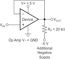
Some applications require output voltage swings from 0 V to a positive full-scale voltage (such as 2.5 V) with excellent accuracy. With most single-supply operational amplifiers, problems arise when the output signal approaches 0 V, near the lower output swing limit of a single-supply operational amplifier. A good single-supply operational amplifier may swing close to single-supply ground, but does not reach ground. The output of the OPA317-Q1, OPA2317-Q1, and OPA4317-Q1 can be made to swing to ground, or slightly below, on a single-supply power source. To do so requires the use of another resistor and an additional, more negative power supply than the operational amplifier negative supply. A pulldown resistor can be connected between the output and the additional negative supply to pull the output down below the value that the output would otherwise achieve, as shown in Figure 21.
 Figure 21. For VOUT Range to Ground
The OPA317-Q1, OPA2317-Q1, and OPA4317-Q1 have an output stage that allows the output voltage to be pulled to its negative supply rail, or slightly below, using the technique previously described. This technique only works with some types of output stages. The OPA317-Q1, OPA2317-Q1, and OPA4317-Q1 have been characterized to perform with this technique; the recommended resistor value is approximately 20 kΩ. This configuration increases the current consumption by several hundreds of microamps. Accuracy is excellent down to 0 V and as low as –2 mV. Limiting and nonlinearity occur below –2 mV, but excellent accuracy returns as the output drives back up above –2 mV. Lowering the resistance of the pulldown resistor allows the operational amplifier to swing even further below the negative rail. Use resistances as low as 10 kΩ to achieve excellent accuracy down to –10 mV.
9.2 Typical Applications
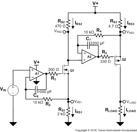
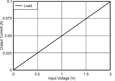
The circuit shown in Figure 22 is a high-side voltage-to-current (V-I) converter. It translates an input voltage of 0 V to 2 V to an output current of 0 mA to 100 mA. Figure 23 shows the measured transfer function for this circuit. The low offset voltage and offset drift of the OPA317 facilitate excellent DC accuracy for the circuit.
 Figure 22. High-Side Voltage-to-Current (V-I) Converter
9.2.1 Design Requirements
The design requirements are as follows:
- Supply Voltage: 5-V DC
- Input: 0-V to 2-V DC
- Output: 0-mA to 100-mA DC
9.2.2 Detailed Design Procedure
The V-I transfer function of the circuit is based on the relationship between the input voltage, VIN, and the three current-sensing resistors: RS1, RS2, and RS3. The relationship between VIN and RS1 determines the current that flows through the first stage of the design. The current gain from the first stage to the second stage is based on the relationship between RS2 and RS3.
For a successful design, pay close attention to the DC characteristics of the operational amplifier chosen for the application. To meet the performance goals, this application benefits from an operational amplifier with low offset voltage, low temperature drift, and rail-to-rail output. The OPA2317 CMOS operational amplifier is a high-precision, 5-µV offset, 0.05-μV/°C drift amplifier optimized for low-voltage, single-supply operation with an output swing to within 50 mV of the positive rail. The OPA2317 family uses chopping techniques to provide low initial offset voltage and near-zero drift over time and temperature. Low offset voltage and low drift reduce the offset error in the system, making these devices appropriate for precise DC control. The rail-to-rail output stage of the OPA2317 ensures that the output swing of the operational amplifier is able to fully control the gate of the MOSFET devices within the supply rails.
9.2.3 Application Curve
 Figure 23. Measured Transfer Function for High-Side V-I Converter
9.3 System Example
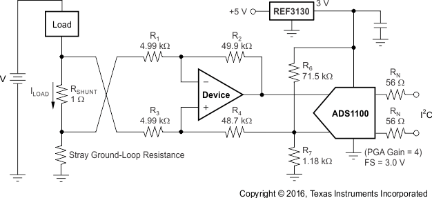
RN are operational resistors used to isolate the ADS1100 from the noise of the digital I2C bus. The ADS1100 device is a 16-bit converter; therefore, a precise reference is essential for maximum accuracy. If absolute accuracy is not required and the 5-V power supply is sufficiently stable, the REF3130 device may be omitted.

NOINDENT:
NOTE: 1% resistors provide adequate common-mode rejection at small ground-loop errors.