ZHCSFA4 July   2016 OPA2317-Q1 , OPA317-Q1

PRODUCTION DATA.  

  1. 特性
  2. 应用
  3. 说明
  4. 修订历史记录
  5. Pin Configuration and Functions
  6. Specifications
    1. 6.1 Absolute Maximum Ratings
    2. 6.2 ESD Ratings
    3. 6.3 Recommended Operating Conditions
    4. 6.4 Thermal Information: OPA317-Q1
    5. 6.5 Thermal Information: OPA2317-Q1
    6. 6.6 Thermal Information: OPA4317-Q1
    7. 6.7 Electrical Characteristics: VS = 1.8 V to 5.5 V
    8. 6.8 Typical Characteristics
  7. Parameter Measurement Information
  8. Detailed Description
    1. 8.1 Overview
    2. 8.2 Functional Block Diagram
    3. 8.3 Feature Description
      1. 8.3.1 Operating Voltage
      2. 8.3.2 Input Voltage
      3. 8.3.3 Input Differential Voltage
      4. 8.3.4 Internal Offset Correction
      5. 8.3.5 EMI Susceptibility and Input Filtering
    4. 8.4 Device Functional Modes
  9. Application and Implementation
    1. 9.1 Application Information
      1. 9.1.1 Achieving Output Swing to the Op Amp Negative Rail
    2. 9.2 Typical Applications
      1. 9.2.1 Design Requirements
      2. 9.2.2 Detailed Design Procedure
      3. 9.2.3 Application Curve
    3. 9.3 System Example
  10. 10Power Supply Recommendations
  11. 11Layout
    1. 11.1 Layout Guidelines
    2. 11.2 Layout Example
  12. 12器件和文档支持
    1. 12.1 文档支持
      1. 12.1.1 相关文档 
    2. 12.2 接收文档更新通知
    3. 12.3 相关链接
    4. 12.4 社区资源
    5. 12.5 商标
    6. 12.6 静电放电警告
    7. 12.7 Glossary
  13. 13机械、封装和可订购信息

封装选项

机械数据 (封装 | 引脚)
散热焊盘机械数据 (封装 | 引脚)
订购信息

11 Layout

11.1 Layout Guidelines

Attention to good layout practice is always recommended. Keep traces short and, when possible, use a printed-circuit board (PCB) ground plane with surface-mount components placed as close to the device pins as possible. Place a 0.1-μF capacitor closely across the supply pins. Apply these guidelines throughout the analog circuit to improve performance and provide benefits, such as reducing the electromagnetic interference (EMI) susceptibility.

Optimize circuit layout and mechanical conditions for lowest offset voltage and precision performance. Avoid temperature gradients that create thermoelectric (Seebeck) effects in the thermocouple junctions formed from connecting dissimilar conductors. These thermally-generated potentials can be made to cancel by assuring they are equal on both input terminals. Other layout and design considerations include:

  • Use low thermoelectric-coefficient conditions (avoid dissimilar metals).
  • Thermally isolate components from power supplies or other heat sources.
  • Shield operational amplifier and input circuitry from air currents, such as cooling fans.

Following these guidelines reduces the likelihood of junctions being at different temperatures, which can cause thermoelectric voltage drift of 0.1 μV/°C or higher, depending on the materials used.

11.2 Layout Example
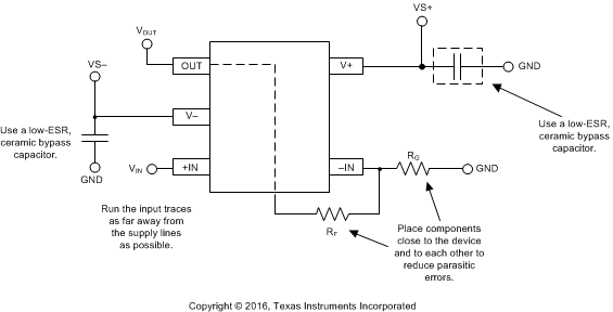
OPA317-Q1 OPA2317-Q1 OPA4317-Q1 SOT_layout_example_SBOS682.gif Figure 25. OPAx317-Q1 Layout Example