ZHCSCS6B September   2014  – December 2018 OPA2320-Q1 , OPA320-Q1

PRODUCTION DATA.  

  1. 特性
  2. 应用
  3. 说明
    1.     零交叉失真:低偏移电压
  4. 修订历史记录
  5. Pin Configuration and Functions
    1.     Pin Functions
  6. Specifications
    1. 6.1 Absolute Maximum Ratings
    2. 6.2 ESD Ratings
    3. 6.3 Recommended Operating Conditions
    4. 6.4 Thermal Information
    5. 6.5 Electrical Characteristics:
    6. 6.6 Typical Characteristics
  7. Detailed Description
    1. 7.1 Overview
    2. 7.2 Functional Block Diagram
    3. 7.3 Feature Description
      1. 7.3.1 Input and ESD Protection
      2. 7.3.2 Feedback Capacitor Improves Response
      3. 7.3.3 EMI Susceptibility And Input Filtering
      4. 7.3.4 Output Impedance
      5. 7.3.5 Capacitive Load and Stability
      6. 7.3.6 Overload Recovery Time
    4. 7.4 Device Functional Modes
      1. 7.4.1 Rail-to-Rail Input
      2. 7.4.2 Phase Reversal
  8. Application and Implementation
    1. 8.1 Application Information
    2. 8.2 Typical Applications
      1. 8.2.1 Transimpedance Amplifier
        1. 8.2.1.1 Design Requirements
        2. 8.2.1.2 Detailed Design Procedure
          1. 8.2.1.2.1 Optimizing The Transimpedance Circuit
        3. 8.2.1.3 Application Curves
      2. 8.2.2 High-Impedance Sensor Interface
      3. 8.2.3 Driving ADCs
      4. 8.2.4 Active Filter
  9. Power Supply Recommendations
  10. 10Layout
    1. 10.1 Layout Guidelines
    2. 10.2 Layout Example
  11. 11器件和文档支持
    1. 11.1 器件支持
      1. 11.1.1 开发支持
    2. 11.2 相关链接
    3. 11.3 接收文档更新通知
    4. 11.4 社区资源
    5. 11.5 商标
    6. 11.6 静电放电警告
    7. 11.7 术语表
  12. 12机械、封装和可订购信息

封装选项

机械数据 (封装 | 引脚)
散热焊盘机械数据 (封装 | 引脚)
订购信息

Driving ADCs

The OPAx320-Q1 series op amps are an excellent choice for driving sampling analog-to-digital converters (ADCs) with sampling speeds up to 1 MSPS. The zero-crossover distortion input stage topology allows the OPAx320-Q1 to drive ADCs without degradation of differential linearity and THD.

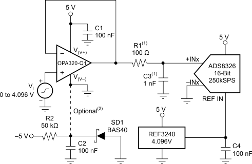
The OPAx320-Q1 can be used to buffer the ADC switched input capacitance and resulting charge injection while providing signal gain. Figure 42 shows the OPAx320-Q1 configured to drive the ADS8326.
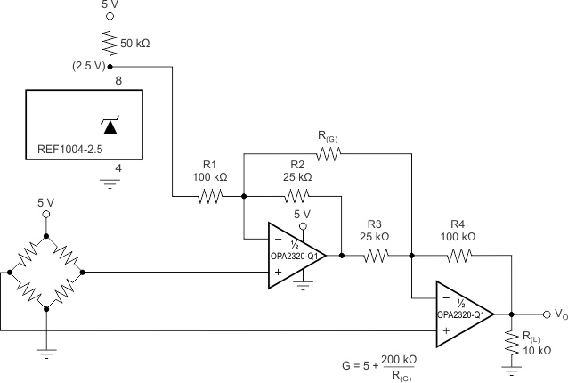
OPA320-Q1 OPA2320-Q1 ai_2opa_hifrq_cmr_slos884.gifFigure 41. Two Op-Amp Instrumentation Amplifier With Improved High-Frequency Common-Mode Rejection
OPA320-Q1 OPA2320-Q1 ai_drv_ads8326_slos884.gif

NOINDENT:

Suggested value; may require adjustment based on specific application.

NOINDENT:

Single-supply applications lose a small number of ADC codes near ground as a result of op amp output swing limitation. If a negative power supply is available, this simple circuit creates a –0.3-V supply to allow output swing to true ground potential.
Figure 42. Driving the ADS8326