SBOS538F January   2011  – December 2016 OPA2322 , OPA322 , OPA4322

PRODUCTION DATA.  

  1. Features
  2. Applications
  3. Description
  4. Revision History
  5. Pin Configuration and Functions
  6. Specifications
    1. 6.1 Absolute Maximum Ratings
    2. 6.2 ESD Ratings
    3. 6.3 Recommended Operating Conditions
    4. 6.4 Thermal Information: OPA322, OPA322S
    5. 6.5 Thermal Information: OPA2322, OPA2322S
    6. 6.6 Thermal Information: OPA4322, OPA4322S
    7. 6.7 Electrical Characteristics
    8. 6.8 Typical Characteristics
  7. Detailed Description
    1. 7.1 Overview
    2. 7.2 Functional Block Diagram
    3. 7.3 Feature Description
      1. 7.3.1 Operating Voltage
      2. 7.3.2 Input and ESD Protection
      3. 7.3.3 Phase Reversal
      4. 7.3.4 Feedback Capacitor Improves Response
      5. 7.3.5 EMI Susceptibility and Input Filtering
      6. 7.3.6 Output Impedance
      7. 7.3.7 Capacitive Load and Stability
      8. 7.3.8 Overload Recovery Time
      9. 7.3.9 Shutdown Function
    4. 7.4 Device Functional Modes
  8. Application and Implementation
    1. 8.1 Application Information
      1. 8.1.1 Active Filter
    2. 8.2 Typical Application
      1. 8.2.1 Design Requirements
      2. 8.2.2 Detailed Design Procedure
      3. 8.2.3 Application Curve
  9. Power Supply Recommendations
  10. 10Layout
    1. 10.1 Layout Guidelines
      1. 10.1.1 Leadless DFN Package
    2. 10.2 Layout Example
  11. 11Device and Documentation Support
    1. 11.1 Device Support
      1. 11.1.1 Third-Party Products Disclaimer
      2. 11.1.2 Development Support
        1. 11.1.2.1 TINA-TI™ (Free Software Download)
        2. 11.1.2.2 DIP Adapter EVM
        3. 11.1.2.3 Universal Operational Amplifier EVM
        4. 11.1.2.4 TI Precision Designs
        5. 11.1.2.5 WEBENCH Filter Designer
    2. 11.2 Documentation Support
      1. 11.2.1 Related Documentation
    3. 11.3 Related Links
    4. 11.4 Receiving Notification of Documentation Updates
    5. 11.5 Community Resources
    6. 11.6 Trademarks
    7. 11.7 Electrostatic Discharge Caution
    8. 11.8 Glossary
  12. 12Mechanical, Packaging, and Orderable Information

封装选项

机械数据 (封装 | 引脚)
散热焊盘机械数据 (封装 | 引脚)
订购信息

Features

  • Gain Bandwidth: 20 MHz
  • Low Noise: 8.5 nV√Hz at 1 kHz
  • Slew Rate: 10 V/μs
  • Low THD+N: 0.0005%
  • Rail-to-Rail I/O
  • Offset Voltage: 2 mV (maximum)
  • Supply Voltage: 1.8 V to 5.5 V
  • Supply Current: 1.5 mA/ch
    • Shutdown: 0.1 μA/ch
  • Unity-Gain Stable
  • Small Packages:
    • SOT-23, SON, VSSOP, TSSOP

Applications

  • Sensor Signal Conditioning
  • Consumer Audio
  • Multi-Pole Active Filters
  • Control-Loop Amplifiers
  • Communications
  • Security
  • Scanners

Zero-Crossover Rail-to-Rail Input Stage Eliminates Distortion
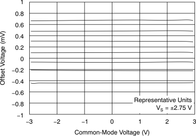
OPA322 OPA322S OPA2322 OPA2322S OPA4322 OPA4322S tc_voff-vcm_bos538.gif

Description

The OPAx322x series consists of single, dual, and quad-channel CMOS operational amplifiers featuring low noise and rail-to-rail inputs and outputs optimized for low-power, single-supply applications. Specified over a wide supply range of 1.8 V to 5.5 V, the low quiescent current of only 1.5 mA per channel makes these devices well-suited for power-sensitive applications.

The combination of very low noise (8.5 nV√Hz at
1 kHz), high-gain bandwidth (20 MHz), and fast slew rate (10 V/μs) make the OPAx322x family ideal for a wide range of applications, including signal conditioning and sensor amplification requiring high gains. Featuring low THD+N, the OPAx322x series is also excellent for consumer audio applications, particularly for single-supply systems.

The OPAx322S models include a shutdown mode that allow the amplifiers to be switched from normal operation to a standby current that is typically less than 0.1 μA.

The OPA322 (single version) is available in 5-pin SOT-23 and 6-pin SOT-23, while the OPA2322 (dual version) is offered in 8-pin VSSOP, 10-pin VSSOP, 8-pin SOIC, and 8-pin SON packages. The quad version OPA4322 comes in 14-pin TSSOP and 16-pin TSSOP packages. All versions are specified for operation from –40°C to +125°C.

Device Information(1)

PART NUMBER PACKAGE BODY SIZE (NOM)
OPA322 SOT-23 (5) 2.90 mm × 1.60 mm
OPA322S SOT-23 (6) 2.90 mm × 1.60 mm
OPA2322 SOIC (8) 4.90 mm × 3.91 mm
VSSOP (8) 3.00 mm × 3.00 mm
SON (8) 3.00 mm × 3.00 mm
OPA2322S VSSOP (10) 3.00 mm × 3.00 mm
OPA4322 TSSOP (14) 5.00 mm × 4.40 mm
OPA4322S TSSOP (16) 5.00 mm × 4.40 mm
  1. For all available packages, see the orderable addendum at the end of the data sheet.