SBOS522A June 2010 – November 2019 OPA333-Q1
PRODUCTION DATA.
- 1 Features
- 2 Applications
- 3 Description
- 4 Revision History
- 5 Pin Configuration and Functions
- 6 Specifications
- 7 Detailed Description
-
8 Application and Implementation
- 8.1 Application Information
- 8.2
Typical Applications
- 8.2.1 High-Side Voltage-to-Current (V-I) Converter
- 8.2.2 Precision, Low-Level Voltage-to-Current (V-I) Converter
- 8.2.3 Composite Amplifier
- 8.2.4 Temperature Measurement
- 8.2.5 Single Op-Amp Bridge-Amplifier
- 8.2.6 Low-Side Current-Monitor
- 8.2.7 High-Side Current Monitor
- 8.2.8 Thermistor Measurement
- 8.2.9 Precision Instrumentation Amplifier
- 9 Power Supply Recommendations
- 10Layout
- 11Device and Documentation Support
- 12Mechanical, Packaging, and Orderable Information
8.1.1 Achieving Output Swing to the Op Amp Negative Rail
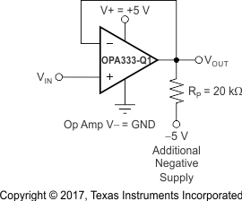
Some applications require output voltage swings from 0 V to a positive full-scale voltage (such as 2.5 V) with excellent accuracy. With most single-supply op amps, problems arise when the output signal approaches 0 V, near the lower output swing limit of a single-supply op amp. A good single-supply op amp may swing close to single-supply ground, but will not reach ground. The output of the OPA333-Q1 can be made to swing to ground, or slightly below, on a single-supply power source. To do so requires the use of another resistor and an additional, more negative, power supply than the op amp negative supply. A pulldown resistor may be connected between the output and the additional negative supply to pull the output down below the value that the output would otherwise achieve (see Figure 19).
 Figure 19. VOUT Range to Ground
 The OPA333-Q1 has an output stage that allows the output voltage to be pulled to its negative supply rail, or slightly below, using the technique previously described. This technique only works with some types of output stages. The OPA333-Q1 has been characterized to perform with this technique; however, the recommended resistor value is approximately 20 kΩ.
NOTE
This configuration increases the current consumption by several hundreds of microamps.
Accuracy is excellent down to 0 V and as low as –2 mV. Limiting and nonlinearity occur below –2 mV, but excellent accuracy returns when the output is again driven above –2 mV. Lowering the resistance of the pulldown resistor allows the op amp to swing even further below the negative rail. Resistors as low as 10 kΩ can be used to achieve excellent accuracy down to –10 mV.