SBOS522A June 2010 – November 2019 OPA333-Q1
PRODUCTION DATA.
- 1 Features
- 2 Applications
- 3 Description
- 4 Revision History
- 5 Pin Configuration and Functions
- 6 Specifications
- 7 Detailed Description
-
8 Application and Implementation
- 8.1 Application Information
- 8.2
Typical Applications
- 8.2.1 High-Side Voltage-to-Current (V-I) Converter
- 8.2.2 Precision, Low-Level Voltage-to-Current (V-I) Converter
- 8.2.3 Composite Amplifier
- 8.2.4 Temperature Measurement
- 8.2.5 Single Op-Amp Bridge-Amplifier
- 8.2.6 Low-Side Current-Monitor
- 8.2.7 High-Side Current Monitor
- 8.2.8 Thermistor Measurement
- 8.2.9 Precision Instrumentation Amplifier
- 9 Power Supply Recommendations
- 10Layout
- 11Device and Documentation Support
- 12Mechanical, Packaging, and Orderable Information
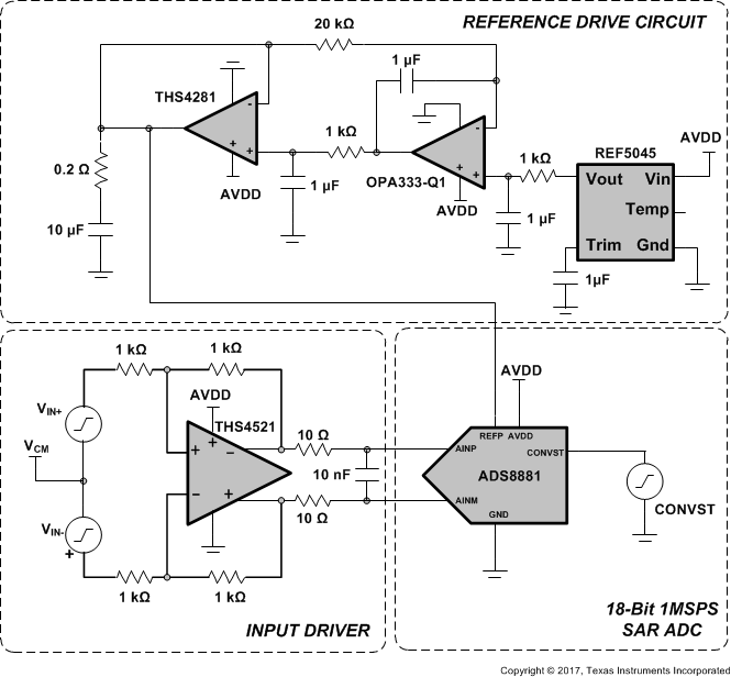
8.2.3 Composite Amplifier
The circuit shown in Figure 25 is a composite amplifier used to drive the reference on the ADS8881. The OPA333-Q1 provides excellent dc accuracy, and the THS4281 allows the output of the circuit to respond quickly to the transient current requirements of a typical successive approximation register (SAR) data-converter reference input. The ADS8881 system was optimized for THD and achieved a measured performance of –110 dB. The linearity of the ADC is shown Figure 26.
 Figure 25. Composite Amplifier Reference Driver Circuit