SBOS522A June   2010  – November 2019 OPA333-Q1

PRODUCTION DATA.  

  1. Features
  2. Applications
  3. Description
    1.     Device Images
      1.      0.1-Hz to 10-Hz Noise
  4. Revision History
  5. Pin Configuration and Functions
    1.     Pin Functions
  6. Specifications
    1. 6.1 Absolute Maximum Ratings
    2. 6.2 ESD Ratings
    3. 6.3 Recommended Operating Conditions
    4. 6.4 Thermal Information
    5. 6.5 Electrical Characteristics
    6. 6.6 Typical Characteristics
  7. Detailed Description
    1. 7.1 Overview
    2. 7.2 Functional Block Diagram
    3. 7.3 Feature Description
      1. 7.3.1 Rail-to-Rail Input Voltage
      2. 7.3.2 Internal Offset Correction
    4. 7.4 Device Functional Modes
  8. Application and Implementation
    1. 8.1 Application Information
      1. 8.1.1 Achieving Output Swing to the Op Amp Negative Rail
    2. 8.2 Typical Applications
      1. 8.2.1 High-Side Voltage-to-Current (V-I) Converter
        1. 8.2.1.1 Design Requirements
        2. 8.2.1.2 Detailed Design Procedure
        3. 8.2.1.3 Application Curve
      2. 8.2.2 Precision, Low-Level Voltage-to-Current (V-I) Converter
        1. 8.2.2.1 Design Requirements
        2. 8.2.2.2 Detailed Design Procedure
        3. 8.2.2.3 Application Curves
      3. 8.2.3 Composite Amplifier
        1. 8.2.3.1 Design Requirements
        2. 8.2.3.2 Detailed Design Procedure
        3. 8.2.3.3 Application Curve
      4. 8.2.4 Temperature Measurement
      5. 8.2.5 Single Op-Amp Bridge-Amplifier
      6. 8.2.6 Low-Side Current-Monitor
      7. 8.2.7 High-Side Current Monitor
      8. 8.2.8 Thermistor Measurement
      9. 8.2.9 Precision Instrumentation Amplifier
  9. Power Supply Recommendations
  10. 10Layout
    1. 10.1 Layout Guidelines
    2. 10.2 Layout Example
  11. 11Device and Documentation Support
    1. 11.1 Documentation Support
      1. 11.1.1 Related Documentation
    2. 11.2 Receiving Notification of Documentation Updates
    3. 11.3 Support Resources
    4. 11.4 Trademarks
    5. 11.5 Electrostatic Discharge Caution
    6. 11.6 Glossary
  12. 12Mechanical, Packaging, and Orderable Information

封装选项

机械数据 (封装 | 引脚)
散热焊盘机械数据 (封装 | 引脚)
订购信息

Low-Side Current-Monitor

A low-side current shunt monitor is shown in Figure 29. The R1 through R6 resistors are operational resistors used to isolate the 16-bit ADS1115-Q1 converter from the noise of the digital I2C bus.
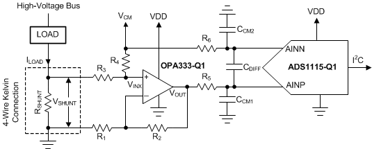
OPA333-Q1 typapp_lowshunt_wrt2p5V_V2_generic_sbas563.gif

NOTE:

1% resistors provide adequate common-mode rejection at small ground-loop errors.
Figure 29. Low-Side Current-Monitor