SBOS522A June   2010  – November 2019 OPA333-Q1

PRODUCTION DATA.  

  1. Features
  2. Applications
  3. Description
    1.     Device Images
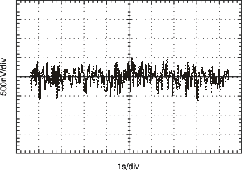
      1.      0.1-Hz to 10-Hz Noise
  4. Revision History
  5. Pin Configuration and Functions
    1.     Pin Functions
  6. Specifications
    1. 6.1 Absolute Maximum Ratings
    2. 6.2 ESD Ratings
    3. 6.3 Recommended Operating Conditions
    4. 6.4 Thermal Information
    5. 6.5 Electrical Characteristics
    6. 6.6 Typical Characteristics
  7. Detailed Description
    1. 7.1 Overview
    2. 7.2 Functional Block Diagram
    3. 7.3 Feature Description
      1. 7.3.1 Rail-to-Rail Input Voltage
      2. 7.3.2 Internal Offset Correction
    4. 7.4 Device Functional Modes
  8. Application and Implementation
    1. 8.1 Application Information
      1. 8.1.1 Achieving Output Swing to the Op Amp Negative Rail
    2. 8.2 Typical Applications
      1. 8.2.1 High-Side Voltage-to-Current (V-I) Converter
        1. 8.2.1.1 Design Requirements
        2. 8.2.1.2 Detailed Design Procedure
        3. 8.2.1.3 Application Curve
      2. 8.2.2 Precision, Low-Level Voltage-to-Current (V-I) Converter
        1. 8.2.2.1 Design Requirements
        2. 8.2.2.2 Detailed Design Procedure
        3. 8.2.2.3 Application Curves
      3. 8.2.3 Composite Amplifier
        1. 8.2.3.1 Design Requirements
        2. 8.2.3.2 Detailed Design Procedure
        3. 8.2.3.3 Application Curve
      4. 8.2.4 Temperature Measurement
      5. 8.2.5 Single Op-Amp Bridge-Amplifier
      6. 8.2.6 Low-Side Current-Monitor
      7. 8.2.7 High-Side Current Monitor
      8. 8.2.8 Thermistor Measurement
      9. 8.2.9 Precision Instrumentation Amplifier
  9. Power Supply Recommendations
  10. 10Layout
    1. 10.1 Layout Guidelines
    2. 10.2 Layout Example
  11. 11Device and Documentation Support
    1. 11.1 Documentation Support
      1. 11.1.1 Related Documentation
    2. 11.2 Receiving Notification of Documentation Updates
    3. 11.3 Support Resources
    4. 11.4 Trademarks
    5. 11.5 Electrostatic Discharge Caution
    6. 11.6 Glossary
  12. 12Mechanical, Packaging, and Orderable Information

封装选项

机械数据 (封装 | 引脚)
散热焊盘机械数据 (封装 | 引脚)
订购信息

Typical Characteristics

at TA = 25°C, VS = 5 V, and CL = 0 pF (unless otherwise noted)
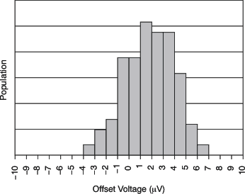
OPA333-Q1 tc_histo_bos351.gif
Figure 1. Offset Voltage Production Distribution
OPA333-Q1 tc_oloop-frq_bos351.gif
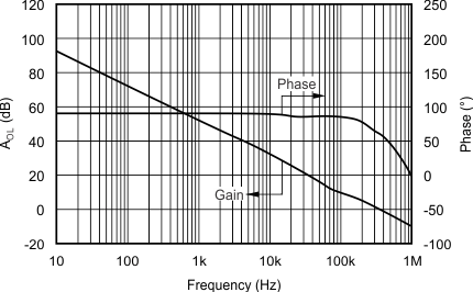
Figure 3. Open-Loop Gain vs Frequency
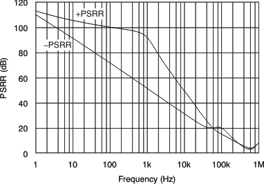
OPA333-Q1 tc_psrr-frq_bos351.gif
Figure 5. Power-Supply Rejection Ratio vs Frequency
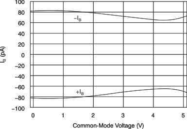
OPA333-Q1 tc_ib-vcm_bos351.gif
VS = 5 V
Figure 7. Input Bias Current vs Common-Mode Voltage
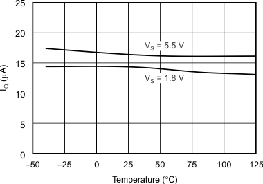
OPA333-Q1 tc_iq-tmp_bos351.gif
Figure 9. Quiescent Current vs Temperature
OPA333-Q1 tc_resp_sm_bos351.gif
G = 1 RL = 10 kΩ
Figure 11. Small-Signal Step Response
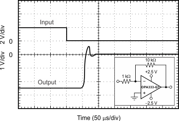
OPA333-Q1 tc_neg_recov_bos522.gif
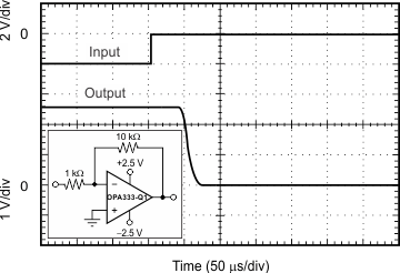
Figure 13. Negative Overvoltage Recovery
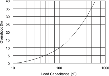
OPA333-Q1 tc_ovrshoot-cl_bos351.gif
Figure 15. Small-Signal Overshoot vs Load Capacitance
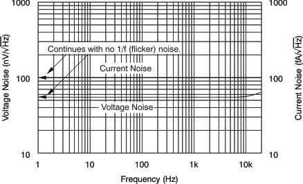
OPA333-Q1 tc_noise-frq_bos351.gif
Figure 17. Current and Voltage Noise Spectral Density vs Frequency
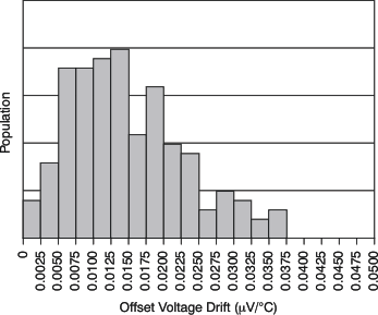
OPA333-Q1 tc_histo_drift_bos351.gif
Figure 2. Offset Voltage Production Distribution
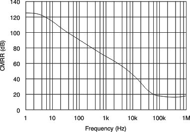
OPA333-Q1 tc_cmrr-frq_bos351.gif
Figure 4. Common-Mode Rejection Ratio vs Frequency
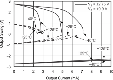
OPA333-Q1 tc_vos-io_bos351.gif
Figure 6. Output Voltage Swing vs Output Current
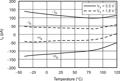
OPA333-Q1 tc_ib-tmp_bos351.gif
Figure 8. Input Bias Current vs Temperature
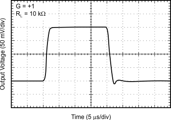
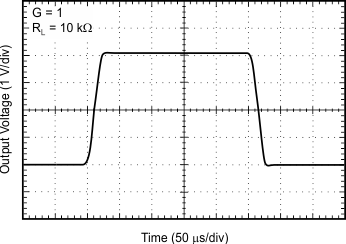
OPA333-Q1 tc_resp_lg_bos351.gif
G = 1 RL = 10 kΩ
Figure 10. Large-Signal Step Response
OPA333-Q1 tc_pos_recov_bos522.gif
Figure 12. Positive Overvoltage Recovery
OPA333-Q1 tc_tim-cloop_bos351.gif
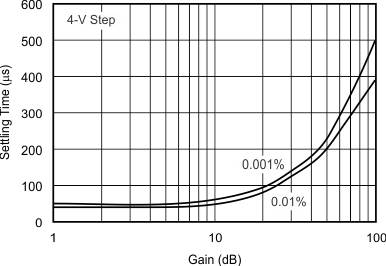
4-V step
Figure 14. Settling Time vs Closed-Loop Gain
OPA333-Q1 tc_noise_bos351.gif
Figure 16. 0.1-Hz to 10-Hz Noise