ZHCSI38E March   2001  – April 2018 OPA2355 , OPA3355 , OPA355

PRODUCTION DATA.  

  1. 特性
  2. 应用
  3. 说明
    1.     Device Images
      1.      简化原理图
  4. 修订历史记录
  5. Device Comparison Table
  6. Pin Configuration and Functions
    1.     Pin Functions: OPA355
    2.     Pin Functions: OPA2355
    3.     Pin Functions: OPA3355
  7. Specifications
    1. 7.1 Absolute Maximum Ratings
    2. 7.2 ESD Ratings
    3. 7.3 Recommended Operating Conditions
    4. 7.4 Thermal Information: OPA355
    5. 7.5 Thermal Information: OPA2355
    6. 7.6 Thermal Information: OPA3355
    7. 7.7 Electrical Characteristics: VS = 2.7 V to 5.5 V (Single-Supply)
    8. 7.8 Typical Characteristics
  8. Detailed Description
    1. 8.1 Overview
    2. 8.2 Functional Block Diagram
    3. 8.3 Feature Description
      1. 8.3.1 Operating Voltage
      2. 8.3.2 Enable Function
      3. 8.3.3 Output Drive
    4. 8.4 Device Functional Modes
  9. Application and Implementation
    1. 9.1 Application Information
    2. 9.2 Typical Applications
      1. 9.2.1 Transimpedance Amplifier
        1. 9.2.1.1 Design Requirements
        2. 9.2.1.2 Detailed Design Procedure
          1. 9.2.1.2.1 Optimizing The Transimpedance Circuit
        3. 9.2.1.3 Application Curve
      2. 9.2.2 High-Impedance Sensor Interface
      3. 9.2.3 Driving ADCs
      4. 9.2.4 Active Filter
    3. 9.3 Video
    4. 9.4 Wideband Video Multiplexing
  10. 10Power Supply Recommendations
  11. 11Layout
    1. 11.1 Layout Guidelines
    2. 11.2 Layout Example
  12. 12器件和文档支持
    1. 12.1 相关链接
    2. 12.2 接收文档更新通知
    3. 12.3 社区资源
    4. 12.4 商标
    5. 12.5 静电放电警告
    6. 12.6 术语表
  13. 13机械、封装和可订购信息

封装选项

机械数据 (封装 | 引脚)
散热焊盘机械数据 (封装 | 引脚)
订购信息

Typical Characteristics

TA = 25°C, VS = 5 V, G = 2, RF = 604 Ω, and RL = 150 Ω connected to VS / 2, (unless otherwise noted)
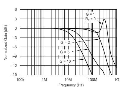
OPA355 OPA2355 OPA3355 Curve01_slos868.gif
VO = 0.1 VP-P
Figure 1. Noninverting Small-Signal Frequency Response
OPA355 OPA2355 OPA3355 Curve03_slos868.gif
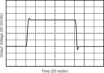
G = 2
Figure 3. Noninverting Small-Signal Step Response
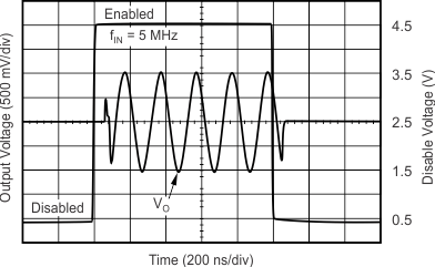
OPA355 OPA2355 OPA3355 Curve05_slos868.gif
Figure 5. Large-Signal Disable and Enable Response
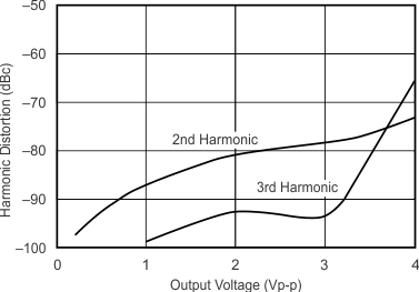
OPA355 OPA2355 OPA3355 Curve07_slos868.gif
RL = 200 ƒ = 1 MHz
Figure 7. Harmonic Distortion vs Output Voltage
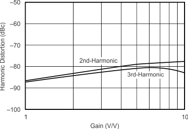
OPA355 OPA2355 OPA3355 Curve09_slos868.gif
RL = 200 VO = 2 VP-P ƒ = 1 MHz
Figure 9. Harmonic Distortion vs Inverting Gain
OPA355 OPA2355 OPA3355 Curve11_slos868.gif
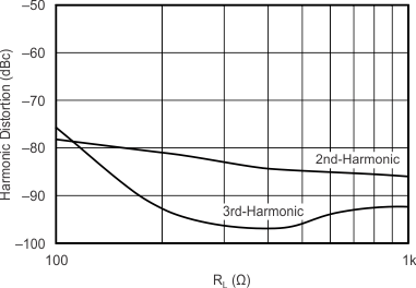
ƒ = 1 MHz VO = 2 VP-P
Figure 11. Harmonic Distortion vs Load Resistance
OPA355 OPA2355 OPA3355 Curve13_sbos195.gif
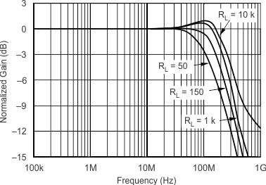
CL = 0 pF VO = 0.1 VP-P
Figure 13. Frequency Response for Various RL Values
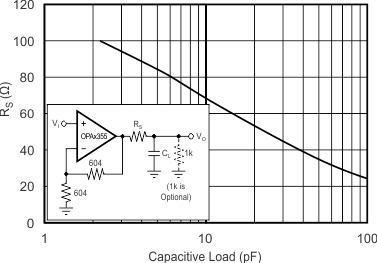
OPA355 OPA2355 OPA3355 Curve15_sbos195.gif
Figure 15. Recommended RS Values vs Capacitive Load
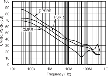
OPA355 OPA2355 OPA3355 Curve17_slos868.gif
Figure 17. Common-Mode Rejection Ratio and Power-Supply Rejection Ratio vs Frequency
OPA355 OPA2355 OPA3355 Curve19_slos868.gif
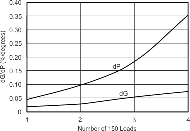
Figure 19. Composite Video Differential Gain and Phase
OPA355 OPA2355 OPA3355 Curve21_slos868.gif
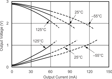
Continuous currents above 60 mA are not recommended
VS = 3 V
Figure 21. Output Voltage Swing vs Output Current
OPA355 OPA2355 OPA3355 Curve23_slos868.gif
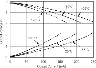
Continuous currents above 60 mA are not recommended
VS = 5 V
Figure 23. Output Voltage Swing vs Output Current
OPA355 OPA2355 OPA3355 Curve25_sbos195.gif
Figure 25. Closed-Loop Output Impedance vs Frequency
OPA355 OPA2355 OPA3355 Curve27_slos868.gif
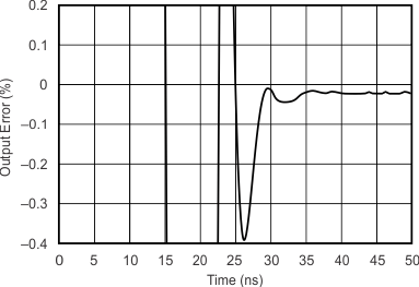
VO = 2 VP-P
Figure 27. Output Settling Time to 0.1%
OPA355 OPA2355 OPA3355 Curve29_slos868.gif
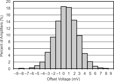
Figure 29. Offset Voltage Production Distribution
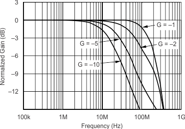
OPA355 OPA2355 OPA3355 Curve02_slos868.gif
VO = 0.1 VP-P
Figure 2. Inverting Small-Signal Frequency Response
OPA355 OPA2355 OPA3355 Curve04_slos868.gif
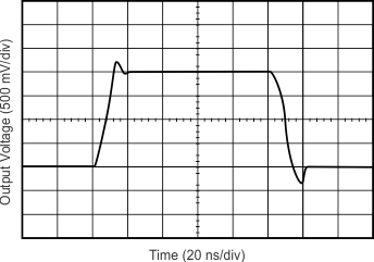
G = 2
Figure 4. Noninverting Large-Signal Step Response
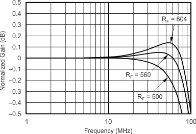
OPA355 OPA2355 OPA3355 Curve06_slos868.gif
CL = 0 pF VO = 0.1 VP-P
Figure 6. 0.1-dB Gain Flatness for Various RF Values
OPA355 OPA2355 OPA3355 Curve08_slos868.gif
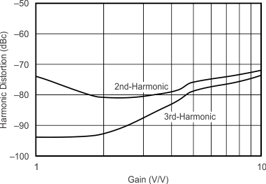
RL = 200 VO = 2 VP-P ƒ = 1 MHz
Figure 8. Harmonic Distortion vs Noninverting Gain
OPA355 OPA2355 OPA3355 Curve10_slos868.gif
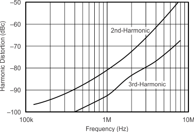
RL = 200 VO = 2 VP-P
Figure 10. Harmonic Distortion vs Frequency
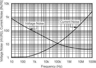
OPA355 OPA2355 OPA3355 Curve12_slos868.gif
Figure 12. Input Voltage and Current Noise Spectral Density vs Frequency
OPA355 OPA2355 OPA3355 Curve14_slos868.gif
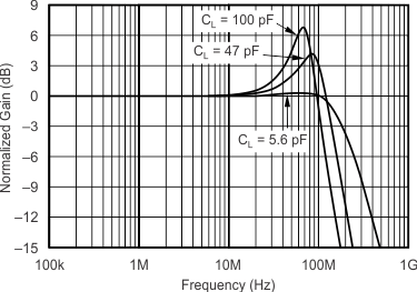
RS = 0 VO = 0.1 VP-P
Figure 14. Frequency Response for Various CL Values
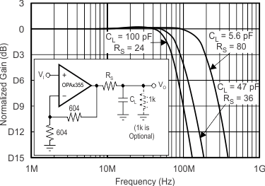
OPA355 OPA2355 OPA3355 Curve16_sbos195.gif
Figure 16. Frequency Response vs Capacitive Load
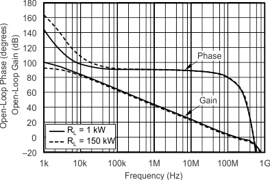
OPA355 OPA2355 OPA3355 Curve18_slos868.gif
Figure 18. Open-Loop Gain and Phase
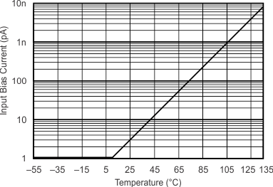
OPA355 OPA2355 OPA3355 Curve20_slos868.gif
Figure 20. Input Bias Current vs Temperature
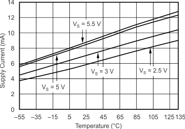
OPA355 OPA2355 OPA3355 Curve22_slos868.gif
Figure 22. Supply Current vs Temperature
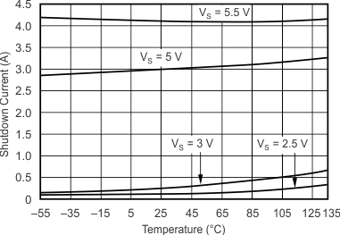
OPA355 OPA2355 OPA3355 Curve24_slos868.gif
Figure 24. Shutdown Current vs Temperature
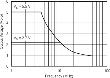
OPA355 OPA2355 OPA3355 Curve26_slos868.gif
Maximum output voltage without slew-rate induced distortion
Figure 26. Maximum Output Voltage vs Frequency
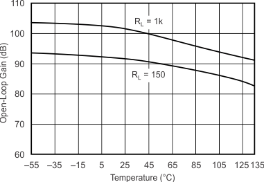
OPA355 OPA2355 OPA3355 Curve28_slos868.gif
Figure 28. Open-Loop Gain vs Temperature
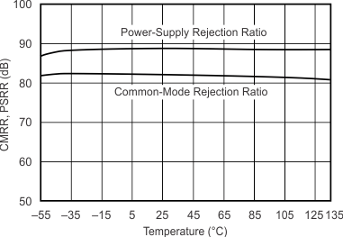
OPA355 OPA2355 OPA3355 Curve30_slos868.gif
Figure 30. Common-Mode Rejection Ratio and Power-Supply Rejection Ratio vs Temperature