ZHCSI38E March 2001 – April 2018 OPA2355 , OPA3355 , OPA355
PRODUCTION DATA.
- 1 特性
- 2 应用
- 3 说明
- 4 修订历史记录
- 5 Device Comparison Table
- 6 Pin Configuration and Functions
- 7 Specifications
- 8 Detailed Description
- 9 Application and Implementation
- 10Power Supply Recommendations
- 11Layout
- 12器件和文档支持
- 13机械、封装和可订购信息
6 Pin Configuration and Functions
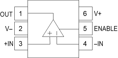
OPA355 DBV Package
6-Pin SOT-23
Top View

1. Pin 1 of the SOT-23-6 is determined by orienting the package marking as indicated in the diagram.
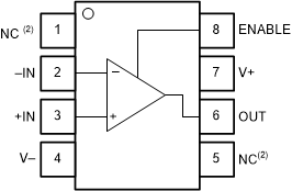
OPA355 D Package
8-Pin SOIC
Top View

1. Pin 1 of the SOT-23-6 is determined by orienting the package marking as indicated in the diagram.
2. NC - no internal connection
Pin Functions: OPA355
| PIN | I/O | DESCRIPTION | ||
|---|---|---|---|---|
| NAME | SOT-23 | SOIC | ||
| ENABLE | 5 | 8 | — | Amplifier power down.
Low = disabled, high = normal operation (pin must be driven) |
| IN+ | 3 | 3 | I | Noninverting input pin |
| IN– | 4 | 2 | I | Inverting input pin |
| NC | — | 1,5 | — | Do not connect. |
| OUT | 1 | 6 | O | Output pin |
| V+ | 6 | 7 | — | Positive power supply |
| V– | 2 | 4 | — | Negative power supply |
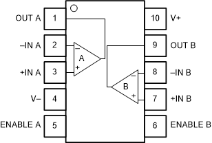
OPA2355 DGS Package
10-Pin VSSOP
Top View

Pin Functions: OPA2355
| PIN | I/O | DESCRIPTION | |
|---|---|---|---|
| NAME | NO. | ||
| ENABLE A | 5 | — | Amplifier power down, channel A.
Low = disabled, high = normal operation (pin must be driven) |
| ENABLE B | 6 | — | Amplifier power down, channel B.
Low = disabled, high = normal operation (pin must be driven) |
| +IN A | 3 | I | Noninverting input pin, channel A |
| +IN B | 7 | I | Noninverting input pin, channel B |
| –IN A | 2 | I | Inverting input pin, channel A |
| –IN B | 8 | I | Inverting input pin, channel B |
| OUT A | 1 | O | Output pin, channel A |
| OUT B | 9 | O | Output pin, channel B |
| V+ | 10 | — | Positive power supply |
| V– | 4 | — | Negative power supply |
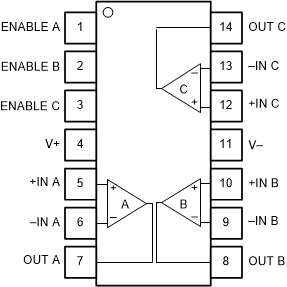
OPA3355 D and PW Packages
14-Pin SOIC, TSSOP
Top View

Pin Functions: OPA3355
| PIN | I/O | DESCRIPTION | |
|---|---|---|---|
| NAME | NO. | ||
| ENABLE A | 1 | — | Amplifier power down, channel A.
Low = disabled, high = normal operation (pin must be driven) |
| ENABLE B | 2 | — | Amplifier power down, channel B.
Low = disabled, high = normal operation (pin must be driven) |
| ENABLE C | 3 | — | Amplifier power down, channel C.
Low = disabled, high = normal operation (pin must be driven) |
| +IN A | 5 | I | Noninverting input pin, channel A |
| +IN B | 10 | I | Noninverting input pin, channel B |
| +IN C | 12 | I | Noninverting input pin, channel C |
| –IN A | 6 | I | Inverting input pin, channel A |
| –IN B | 9 | I | Inverting input pin, channel B |
| –IN C | 13 | I | Inverting input pin, channel C |
| OUT A | 7 | O | Output, channel A |
| OUT B | 8 | O | Output channel B |
| OUT C | 14 | O | Output, channel C |
| V+ | 4 | — | Positive power supply |
| V– | 11 | — | Negative power supply |