ZHCSI16F March 2002 – April 2018 OPA2357 , OPA357
PRODUCTION DATA.
- 1 特性
- 2 应用
- 3 说明
- 4 修订历史记录
- 5 Pin Configuration and Functions
- 6 Specifications
-
7 Detailed Description
- 7.1 Overview
- 7.2 Functional Block Diagram
- 7.3
Feature Description
- 7.3.1 OPAx357 Comparison
- 7.3.2 Operating Voltage
- 7.3.3 Enable Function
- 7.3.4 Rail-to-Rail Input
- 7.3.5 Rail-to-Rail Output
- 7.3.6 Output Drive
- 7.3.7 Video
- 7.3.8 Wideband Video Multiplexing
- 7.3.9 Driving Analog-to-Digital Converters
- 7.3.10 Capacitive Load and Stability
- 7.3.11 Wideband Transimpedance Amplifier
- 7.4 Device Functional Modes
- 8 Application and Implementation
- 9 Power Supply Recommendations
- 10Layout
- 11器件和文档支持
- 12机械、封装和可订购信息
8.2.1 Transimpedance Amplifier
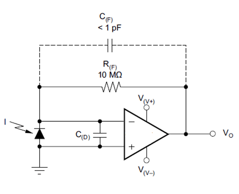
Wide gain bandwidth, low input bias current, low input voltage, and current noise make the OPAx357 family of devices an ideal wideband photodiode transimpedance amplifier. Low-voltage noise is important because photodiode capacitance causes the effective noise gain of the circuit to increase at high frequency. The key elements to a transimpedance design, as shown in Figure 41, are the expected diode capacitance, (which include the parasitic input common-mode and differential-mode input capacitance) the desired transimpedance gain, and the gain-bandwidth (GBW) for the OPAx357 family of devices (20 MHz). With these three variables set, the feedback capacitor value is set to control the frequency response. Feedback capacitance includes the stray capacitance, which is 0.2 pF for a typical surface-mount resistor.
 Figure 41. Dual-Supply Transimpedance Amplifier