ZHCS042C April 2011 – March 2021 OPA2376-Q1 , OPA376-Q1 , OPA4376-Q1
PRODUCTION DATA
- 1 特性
- 2 应用
- 3 说明
- 4 Revision History
- 5 Pin Configuration and Functions
- 6 Specifications
- 7 Detailed Description
- 8 Application and Implementation
- 9 Power Supply Recommendations
- 10Layout
- 11Device and Documentation Support
- 12Mechanical, Packaging, and Orderable Information
7.3.3 Capacitive Load and Stability
The OPAx376-Q1 series of amplifiers may be used in applications where driving a capacitive load is required. As with all op amps, there may be specific instances where the OPAx376-Q1 can become unstable, leading to oscillation. The particular op amp circuit configuration, layout, gain, and output loading are some of the factors to consider when establishing whether an amplifier is be stable in operation. An op amp in the unity-gain (1 V/V) buffer configuration and driving a capacitive load exhibits a greater tendency to be unstable than an amplifier operated at a higher noise gain. The capacitive load, in conjunction with the op amp output resistance, creates a pole within the feedback loop that degrades the phase margin. The degradation of the phase margin increases as the capacitive loading increases.
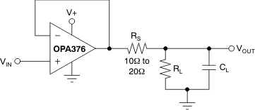
The OPAx376 in a unity-gain configuration can directly drive up to 250 pF of pure capacitive load. Increasing the gain enhances the ability of the amplifier to drive greater capacitive loads; see the typical characteristic plot Figure 6-18, Small-Signal Overshoot vs Load Capacitance. In unity-gain configurations, capacitive load drive can be improved by inserting a small (10-Ω to 20-Ω) resistor, RS, in series with the output, as shown in Figure 7-1. This resistor significantly reduces ringing while maintaining dc performance for purely capacitive loads. However, if there is a resistive load in parallel with the capacitive load, a voltage divider is created, introducing a gain error at the output and slightly reducing the output swing. The error introduced is proportional to the ratio RS / RL, and is generally negligible at low output current levels.
 Figure 7-1 Improving Capacitive Load Drive