SBOS406G June 2007 – December 2015 OPA2376 , OPA376 , OPA4376
PRODUCTION DATA.
- 1 Features
- 2 Applications
- 3 Description
- 4 Revision History
- 5 Pin Configuration and Functions
- 6 Specifications
- 7 Detailed Description
- 8 Application and Implementation
- 9 Power Supply Recommendations
- 10Layout
- 11Device and Documentation Support
- 12Mechanical, Packaging, and Orderable Information
封装选项
机械数据 (封装 | 引脚)
散热焊盘机械数据 (封装 | 引脚)
订购信息
7 Detailed Description
7.1 Overview
The OPA376 family belongs to a new generation of low-noise operational amplifiers with e-trim, giving customers outstanding dc precision and ac performance. Low noise, rail-to-rail input and output, and low offset, drawing a low quiescent current, make these devices ideal for a variety of precision and portable applications. In addition, this device has a wide supply range with excellent PSRR, making it a suitable option for applications that are battery-powered without regulation.
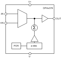
7.2 Functional Block Diagram

7.3 Feature Description
The OPAx376 family of precision amplifiers offers excellent dc performance as well as excellent ac performance. Operating from a single power-supply the OPAx376 is capable of driving large capacitive loads, has a wide input common-mode voltage range, and is well-suited to drive the inputs of SAR ADCs as well as 24-bit and higher resolution converters. Including internal ESD protection, the OPAx376 family is offered in a variety of industry-standard packages, including a wafer chip-scale package for applications that require space savings.
7.3.1 Operating Voltage
The OPA376 family of amplifiers operates over a power-supply range of 2.2 V to 5.5 V (±1.1 V to ±2.75 V). Many of the specifications apply from –40°C to +125°C. Parameters that can exhibit significant variance with regard to operating voltage or temperature are presented in the Typical Characteristics.
7.3.2 Input Offset Voltage and Input Offset Voltage Drift
The OPAx376 family of operational amplifiers is manufactured using TI's e-trim technology. Each amplifier is trimmed in production, thereby minimizing errors associated with input offset voltage and input offset voltage drift. The e-trim technology is a TI proprietary method of trimming internal device parameters during either wafer probing or final testing.
7.3.3 Capacitive Load and Stability
The OPA376 series of amplifiers may be used in applications where driving a capacitive load is required. As with all op amps, there may be specific instances where the OPAx376 can become unstable, leading to oscillation. The particular op amp circuit configuration, layout, gain, and output loading are some of the factors to consider when establishing whether an amplifier will be stable in operation. An op amp in the unity-gain (+1-V/V) buffer configuration and driving a capacitive load exhibits a greater tendency to be unstable than an amplifier operated at a higher noise gain. The capacitive load, in conjunction with the op amp output resistance, creates a pole within the feedback loop that degrades the phase margin. The degradation of the phase margin increases as the capacitive loading increases.
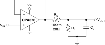
The OPAx376 in a unity-gain configuration can directly drive up to 250 pF of pure capacitive load. Increasing the gain enhances the ability of the amplifier to drive greater capacitive loads; see the typical characteristic Figure 16. In unity-gain configurations, capacitive load drive can be improved by inserting a small (10-Ω to 20-Ω) resistor, RS, in series with the output, as shown in Figure 22. This resistor significantly reduces ringing while maintaining dc performance for purely capacitive loads. However, if there is a resistive load in parallel with the capacitive load, a voltage divider is created, introducing a gain error at the output and slightly reducing the output swing. The error introduced is proportional to the ratio RS / RL, and is generally negligible at low output current levels.
 Figure 22. Improving Capacitive Load Drive
7.3.4 Common-Mode Voltage Range
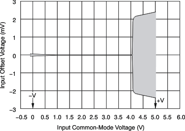
The input common-mode voltage range of the OPA376 series extends 100 mV beyond the supply rails. The offset voltage of the amplifier is very low, from approximately (V–) to (V+) – 1 V, as shown in Figure 23. The offset voltage increases as common-mode voltage exceeds (V+) –1 V. Common-mode rejection is specified from (V–) to (V+) – 1.3 V.
 Figure 23. Offset and Common-Mode Voltage
7.3.5 Input and ESD Protection
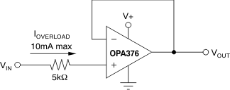
The OPA376 family incorporates internal electrostatic discharge (ESD) protection circuits on all pins. In the case of input and output pins, this protection primarily consists of current steering diodes connected between the input and power-supply pins. These ESD protection diodes also provide in-circuit, input overdrive protection, as long as the current is limited to 10 mA as stated in the Absolute Maximum Ratings. Figure 24 shows how a series input resistor may be added to the driven input to limit the input current. The added resistor contributes thermal noise at the amplifier input and its value should be kept to a minimum in noise-sensitive applications.
 Figure 24. Input Current Protection
7.4 Device Functional Modes
The OPAx376 has a single functional mode and is operational when the power-supply voltage is greater than 2.2 V (±1.1 V). The maximum power supply voltage for the OPAx376 is 5.5 V (±2.75 V).