ZHCSP72A August   2020  – November 2021 OPA2388-Q1 , OPA388-Q1

PRODUCTION DATA  

  1. 特性
  2. 应用
  3. 说明
  4. Revision History
  5. Pin Configuration and Functions
  6. Specifications
    1. 6.1 Absolute Maximum Ratings
    2. 6.2 ESD Ratings
    3. 6.3 Recommended Operating Conditions
    4. 6.4 Thermal Information: OPA388-Q1
    5. 6.5 Thermal Information: OPA2388-Q1
    6. 6.6 Electrical Characteristics
    7. 6.7 Typical Characteristics
  7. Detailed Description
    1. 7.1 Overview
    2. 7.2 Functional Block Diagram
    3. 7.3 Feature Description
      1. 7.3.1 Input Voltage and Zero-Crossover Functionality
      2. 7.3.2 Input Differential Voltage
      3. 7.3.3 Internal Offset Correction
      4. 7.3.4 EMI Susceptibility and Input Filtering
    4. 7.4 Device Functional Modes
  8. Application and Implementation
    1. 8.1 Application Information
    2. 8.2 Typical Application
      1. 8.2.1 Design Requirements
      2. 8.2.2 Detailed Design Procedure
      3. 8.2.3 Application Curve
  9. Power Supply Recommendations
  10. 10Layout
    1. 10.1 Layout Guidelines
    2. 10.2 Layout Example
  11. 11Device and Documentation Support
    1. 11.1 Device Support
      1. 11.1.1 Development Support
        1. 11.1.1.1 TINA-TI™ Simulation Software (Free Download)
        2. 11.1.1.2 PSpice® for TI
        3. 11.1.1.3 TI Precision Designs
    2. 11.2 Documentation Support
      1. 11.2.1 Related Documentation
    3. 11.3 接收文档更新通知
    4. 11.4 支持资源
    5. 11.5 Trademarks
    6. 11.6 Electrostatic Discharge Caution
    7. 11.7 术语表
  12. 12Mechanical, Packaging, and Orderable Information

封装选项

机械数据 (封装 | 引脚)
散热焊盘机械数据 (封装 | 引脚)
订购信息

Pin Configuration and Functions

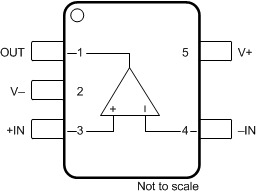
GUID-94080CA9-28F9-4D96-8719-BC1CB4178FF2-low.gifFigure 5-1 OPA388-Q1 DBV (5-Pin SOT-23) Package, Top View
Pin Functions: OPA388-Q1
PIN TYPE DESCRIPTION
NAME NO.
–IN 4 Input Inverting input
+IN 3 Input Noninverting input
NC No internal connection (can be left floating)
OUT 1 Output Output
V– 2 Power Negative (lowest) power supply
V+ 5 Power Positive (highest) power supply
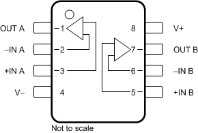
GUID-F2FB334B-6BDF-4E4D-9443-AFABE5EDF844-low.gifFigure 5-2 OPA2388-Q1 D (8-Pin SOIC, Preview) and DGK (8-Pin VSSOP) Packages, Top View
Pin Functions: OPA2388-Q1
PIN TYPE DESCRIPTION
NAME NO.
–IN A 2 Input Inverting input, channel A
–IN B 6 Input Inverting input, channel B
+IN A 3 Input Noninverting input, channel A
+IN B 5 Input Noninverting input, channel B
OUT A 1 Output Output, channel A
OUT B 7 Output Output, channel B
V– 4 Power Negative (lowest) power supply
V+ 8 Power Positive (highest) power supply