VS+ = +2.5 V, VS-= -2.5 V,
RL = 200 Ω, CIN = 4 pF, output load is referenced to
mid-supply, input common-mode biased at mid-supply, and TA ≈ +25°C
(unless otherwise noted)
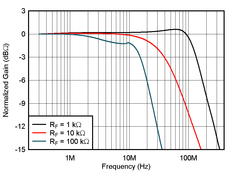
 Figure 6-1 Small-Signal Frequency Response vs Gain
Figure 6-3 Small-Singal Frequency Response vs Ambient Temperature Figure 6-5 Open-Loop Magnitude and Phase vs Frequency Figure 6-7 Large-Signal Crosstalk vs Gain Figure 6-9 Voltage Noise Density vs Ambient Temperature Figure 6-11 Large-Signal Transient
Response Figure 6-13 Output Overload
Reponse − High Gain Setting Figure 6-15 Turn-Off Transient Response Figure 6-17 Quiescent Current (Both
Channels) vs Supply Voltage Figure 6-19 Quiescent Current (Amplifiers Disabled) vs Ambient Temperature Figure 6-21 Offset Voltage vs Ambient Temperature Figure 6-23 Offset Voltage vs Input Common-Mode Voltage vs Ambient
Temperature Figure 6-25 Offset Voltage vs Output Swing vs Ambient Temperature Figure 6-27 Input Bias Current vs Input Common-Mode Voltage Figure 6-29 Output Swing vs Sourcing Current
| µ = 0.450 mV, σ = 0.845 mV |
Figure 6-31 Offset Voltage
Distribution − Channel A
| µ = 0.896 pA, σ = 0.383 pA |
Figure 6-33 Input Bias Current
Distribution − Channel A
| VOUT = 100 mVPP,
RF = 1 kΩ |
Figure 6-2 Small-Signal Frequency Response vs Output LoadFigure 6-4 Large-Signal Frequency Response vs Gain Figure 6-6 Closed-Loop Output Impedance vs Frequency Figure 6-8 Voltage Noise Density vs Frequency Figure 6-10 Small-Signal Transient Response Figure 6-12 Output Overload
Reponse − Low Gain Settings Figure 6-14 Turn-On Transient Response Figure 6-16 Power Supply Rejection Ratio vs Frequency Figure 6-18 Quiescent Current (Both Channels) vs Ambient Temperature Figure 6-20 Offset Voltage vs Supply Voltage Figure 6-22 Offset Voltage vs Input Common-Mode Voltage Figure 6-24 Offset Voltage vs Output Swing Figure 6-26 Input Bias Current vs Ambient Temperature Figure 6-28 Output Swing vs Sinking Current
| µ = 42.2 mA, σ = 0.251 mA |
Figure 6-30 Quiescent Current (Both Channels) Distribution
| µ = 0.606 mV, σ = 0.754 mV |
Figure 6-32 Offset Voltage
Distribution − Channel B
| µ = 0.825 pA, σ = 0.386 pA |
Figure 6-34 Input Bias Current
Distribution − Channel B