ZHCSJA0F June 2010 – March 2023 OPA140 , OPA2140 , OPA4140
PRODUCTION DATA
- 1
- 1 特性
- 2 应用
- 3 说明
- 4 Revision History
- 5 Pin Configuration and Functions
- 6 Specifications
- 7 Detailed Description
- 8 Application and Implementation
- 9 Device and Documentation Support
- 10Mechanical, Packaging, and Orderable Information
6.8 Typical Characteristics
at TA = 25°C, VS = ±18 V, RL = 2 kΩ connected to midsupply, and VCM = VOUT = midsupply (unless otherwise noted)
Table 6-1 Table of Graphs
| DESCRIPTION | FIGURE |
|---|---|
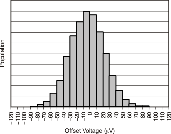
| Offset Voltage Production Distribution | Figure 6-1 |
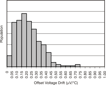
| Offset Voltage Drift Distribution | Figure 6-2 |
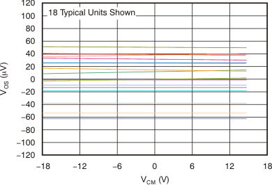
| Offset Voltage vs Common-Mode Voltage (Maximum Supply) | Figure 6-3 |
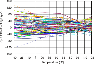
| Input Offset Voltage vs Temperature | Figure 6-4 |
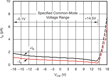
| IB vs Common-Mode Voltage | Figure 6-5 |
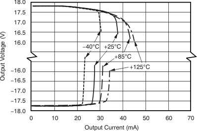
| Output Voltage Swing vs Output Current | Figure 6-6 |
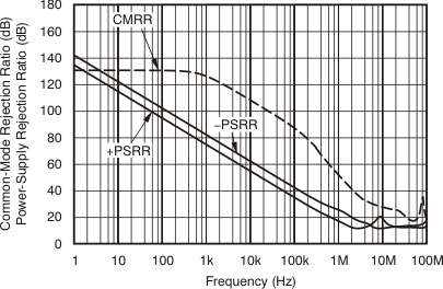
| CMRR and PSRR vs Frequency (RTI) | Figure 6-7 |
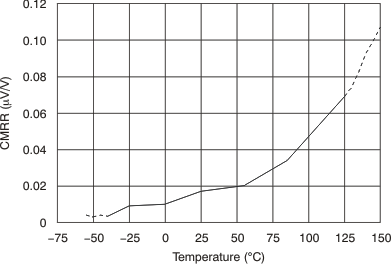
| Common-Mode Rejection Ratio vs Temperature | Figure 6-8 |
| 0.1-Hz to 10-Hz Noise | Figure 6-9 |
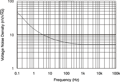
| Input Voltage Noise Density vs Frequency | Figure 6-10 |
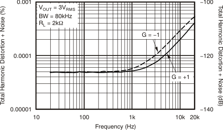
| THD+N Ratio vs Frequency (80-kHz AP Bandwidth) | Figure 6-11 |
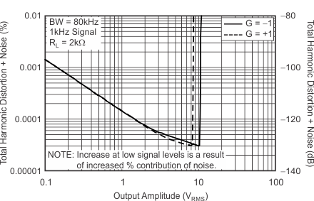
| THD+N Ratio vs Output Amplitude | Figure 6-12 |
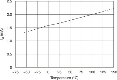
| Quiescent Current vs Temperature | Figure 6-13 |
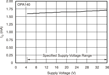
| Quiescent Current vs Supply Voltage | Figure 6-14 |
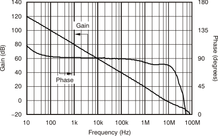
| Gain and Phase vs Frequency | Figure 6-15 |
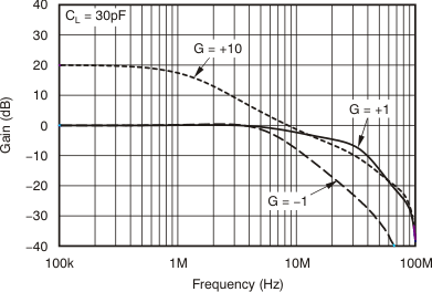
| Closed-Loop Gain vs Frequency | Figure 6-16 |
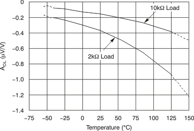
| Open-Loop Gain vs Temperature | Figure 6-17 |
| Open-Loop Output Impedance vs Frequency | Figure 6-18 |
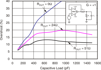
| Small-Signal Overshoot vs Capacitive Load (G = 1) | Figure 6-19 |
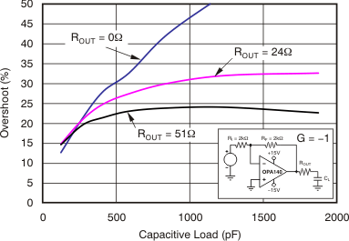
| Small-Signal Overshoot vs Capacitive Load (G = –1) | Figure 6-20 |
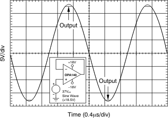
| No Phase Reversal | Figure 6-21 |
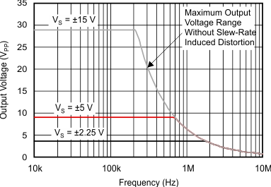
| Maximum Output Voltage vs Frequency | Figure 6-22 |
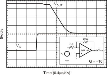
| Positive Overload Recovery | Figure 6-23 |
| Negative Overload Recovery | Figure 6-24 |
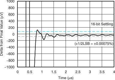
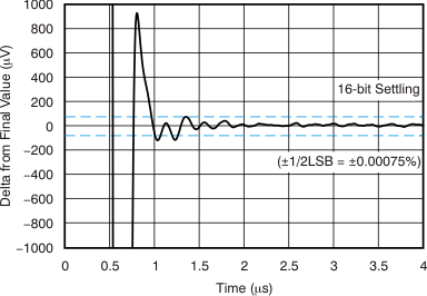
| Large-Signal Positive and Negative Settling Time | Figure 6-25, Figure 6-26 |
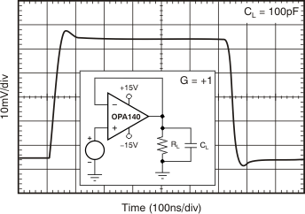
| Small-Signal Step Response (G = 1) | Figure 6-27 |
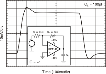
| Small-Signal Step Response (G = –1) | Figure 6-28 |
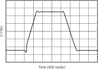
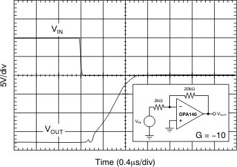
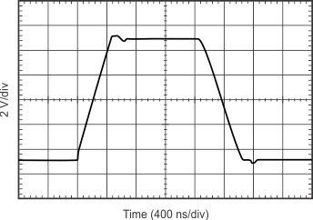
| Large-Signal Step Response (G = 1) | Figure 6-29 |
| Large-Signal Step Response (G = –1) | Figure 6-30 |
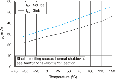
| Short-Circuit Current vs Temperature | Figure 6-31 |
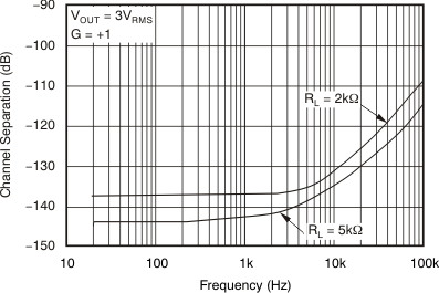
| Channel Separation vs Frequency | Figure 6-32 |
