ZHCSFP9B December   2016  – November 2017 OPA170-Q1 , OPA2170-Q1 , OPA4170-Q1

PRODUCTION DATA.  

  1. 特性
  2. 应用
  3. 说明
    1.     Device Images
      1.      EMIRR IN+ 与频率间的关系
  4. 修订历史记录
  5. Pin Configuration and Functions
    1. Table 1. Pin Functions: OPA170-Q1
    2. Table 2. Pin Functions: OPA2170-Q1
    3. Table 3. Pin Functions: OPA4170-Q1
  6. Specifications
    1. 6.1 Absolute Maximum Ratings
    2. 6.2 ESD Ratings
    3. 6.3 Recommended Operating Conditions
    4. 6.4 Thermal Information: OPA170-Q1
    5. 6.5 Thermal Information: OPA2170-Q1
    6. 6.6 Thermal Information: OPA4170-Q1
    7. 6.7 Electrical Characteristics
    8. 6.8 Typical Characteristics: Table of Graphs
    9. 6.9 Typical Characteristics
  7. Detailed Description
    1. 7.1 Overview
    2. 7.2 Functional Block Diagram
    3. 7.3 Feature Description
      1. 7.3.1 Operating Characteristics
      2. 7.3.2 Phase-Reversal Protection
      3. 7.3.3 Electrical Overstress
      4. 7.3.4 Capacitive Load and Stability
    4. 7.4 Device Functional Modes
      1. 7.4.1 Common-Mode Voltage Range
      2. 7.4.2 Overload Recovery
  8. Application and Implementation
    1. 8.1 Application Information
    2. 8.2 Typical Application
      1. 8.2.1 Design Requirements
      2. 8.2.2 Detailed Design Procedure
      3. 8.2.3 Application Curve
  9. Power Supply Recommendations
  10. 10Layout
    1. 10.1 Layout Guidelines
    2. 10.2 Layout Example
  11. 11器件和文档支持
    1. 11.1 器件支持
      1. 11.1.1 开发支持
        1. 11.1.1.1 TINA-TI™(免费软件下载)
        2. 11.1.1.2 DIP 适配器 EVM
        3. 11.1.1.3 通用运算放大器评估模块 (EVM)
        4. 11.1.1.4 TI 高精度设计
        5. 11.1.1.5 WEBENCH滤波器设计器
    2. 11.2 文档支持
      1. 11.2.1 相关文档
    3. 11.3 相关链接
    4. 11.4 社区资源
    5. 11.5 商标
    6. 11.6 静电放电警告
    7. 11.7 Glossary
  12. 12机械、封装和可订购信息

封装选项

机械数据 (封装 | 引脚)
散热焊盘机械数据 (封装 | 引脚)
订购信息

Detailed Design Procedure

Figure 41 shows a unity-gain buffer driving a capacitive load. Equation 1 shows the transfer function for the circuit in Figure 41. Not shown in Figure 41 is the open-loop output resistance of the operational amplifier, RO.

Equation 1. OPA170-Q1 OPA2170-Q1 OPA4170-Q1 ai_refdes_eqn_bos618.gif

The transfer function in Equation 1 has a pole and a zero. The frequency of the pole (fp) is determined by (RO + RISO) and CLOAD. RISO and CLOAD determine the frequency of the zero (fz). A stable system is obtained by selecting RISO, so the rate of closure (ROC) between the open-loop gain (AOL) and 1/β is 20 dB / decade. Figure 42 depicts the concept. The 1/β curve for a unity-gain buffer is 0 dB.
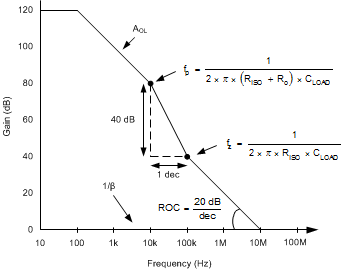
OPA170-Q1 OPA2170-Q1 OPA4170-Q1 ai_refdes_bodeplot_bos618.gifFigure 42. Unity-Gain Amplifier With RISO Compensation

ROC stability analysis is typically simulated. The validity of the analysis depends on multiple factors, especially the accurate modeling of R O . In addition to simulating the ROC, a robust stability analysis includes a measurement of overshoot percentage and ac gain peaking of the circuit using a function generator, oscilloscope, and gain and phase analyzer. Phase margin is then calculated from these measurements. Table 6 shows the overshoot percentage and ac gain peaking that correspond to 45° and 60° phase margins. For more details on this design and other alternative devices that can be used in place of the OPAx170-Q1 family, see Capacitive Load Drive Solution Using an Isolation Resistor.

Table 6. Phase Margin versus Overshoot and AC Gain Peaking

PHASE MARGINOVERSHOOTAC GAIN PEAKING
45° 23.3% 2.35 dB
60° 8.8% 0.28 dB