ZHCSPS9C june   2022  – july 2023 OPA186 , OPA2186 , OPA4186

PRODUCTION DATA  

  1.   1
  2. 特性
  3. 应用
  4. 说明
  5. Revision History
  6. Pin Configuration and Functions
  7. Specifications
    1. 6.1 Absolute Maximum Ratings
    2. 6.2 ESD Ratings
    3. 6.3 Recommended Operating Conditions
    4. 6.4 Thermal Information: OPA186
    5. 6.5 Thermal Information: OPA2186
    6. 6.6 Thermal Information: OPA4186
    7. 6.7 Electrical Characteristics
    8. 6.8 Typical Characteristics
  8. Detailed Description
    1. 7.1 Overview
    2. 7.2 Functional Block Diagram
    3. 7.3 Feature Description
      1. 7.3.1 Rail-to-Rail Inputs
      2. 7.3.2 Phase-Reversal Protection
      3. 7.3.3 Input Bias Current Clock Feedthrough
      4. 7.3.4 EMI Rejection
        1. 7.3.4.1 EMIRR +IN Test Configuration
      5. 7.3.5 Electrical Overstress
      6. 7.3.6 MUX-Friendly Inputs
    4. 7.4 Device Functional Modes
  9. Application and Implementation
    1. 8.1 Application Information
      1. 8.1.1 Basic Noise Calculations
    2. 8.2 Typical Applications
      1. 8.2.1 High-Side Current Sensing
        1. 8.2.1.1 Design Requirements
        2. 8.2.1.2 Detailed Design Procedure
        3. 8.2.1.3 Application Curve
      2. 8.2.2 Bridge Amplifier
    3. 8.3 Power Supply Recommendations
    4. 8.4 Layout
      1. 8.4.1 Layout Guidelines
      2. 8.4.2 Layout Example
  10. Device and Documentation Support
    1. 9.1 Device Support
      1. 9.1.1 Development Support
        1. 9.1.1.1 PSpice® for TI
        2. 9.1.1.2 TINA-TI™ 仿真软件(免费下载)
    2. 9.2 Documentation Support
      1. 9.2.1 Related Documentation
    3. 9.3 接收文档更新通知
    4. 9.4 支持资源
    5. 9.5 Trademarks
    6. 9.6 静电放电警告
    7. 9.7 术语表
  11. 10Mechanical, Packaging, and Orderable Information

封装选项

机械数据 (封装 | 引脚)
散热焊盘机械数据 (封装 | 引脚)
订购信息

Basic Noise Calculations

Low-noise circuit design requires careful analysis of all noise sources. In many cases, external noise sources can dominate; consider the effect of source resistance on overall op-amp noise performance. Total noise of the circuit is the root-sum-square combination of all noise components.

The resistive portion of the source impedance produces thermal noise proportional to the square root of the resistance. The source impedance is usually fixed; consequently, select op amp and the feedback resistors that minimize the respective contributions to the total noise.

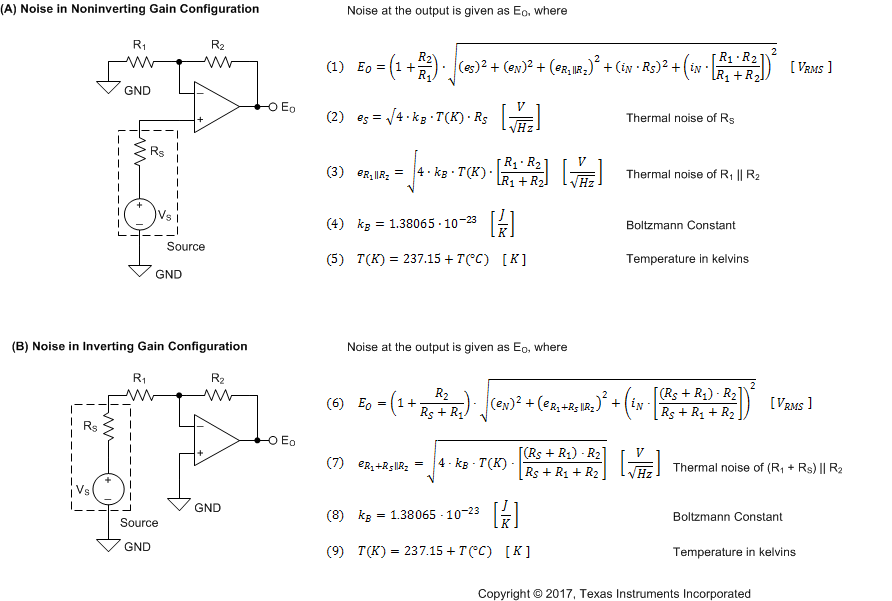
Figure 8-1 shows both noninverting (A) and inverting (B) op-amp circuit configurations with gain. In circuit configurations with gain, the feedback network resistors also contribute noise. In general, the current noise of the op amp reacts with the feedback resistors to create additional noise components. However, the extremely low current noise of the OPAx186 means that the current noise contribution can be ignored.

The feedback resistor values can generally be chosen to make these noise sources negligible. Low impedance feedback resistors load the output of the amplifier. The equations for total noise are shown for both configurations.
GUID-514BDCB1-940D-4221-B345-4521E2BF6A73-low.gif
Where en is the voltage noise spectral density of the amplifier. For the OPAx186 operational amplifier, en = 38 nV/√Hz at 1 kHz.
NOTE: For additional resources on noise calculations, visit TI Precision Labs.
Figure 8-1 Noise Calculation in Gain Configurations