ZHCSFV2D December   2016  – December 2018 OPA187 , OPA2187 , OPA4187

UNLESS OTHERWISE NOTED, this document contains PRODUCTION DATA.  

  1. 特性
  2. 应用
  3. 说明
    1.     Device Images
      1.      OPAx187 具有高精度低侧电流测量功能
  4. 修订历史记录
  5. Pin Configuration and Functions
    1.     Pin Functions: OPA187
    2.     Pin Functions: OPA2187
    3.     Pin Functions: OPA4187
  6. Specifications
    1. 6.1 Absolute Maximum Ratings
    2. 6.2 ESD Ratings
    3. 6.3 Recommended Operating Conditions
    4. 6.4 Thermal Information: OPA187
    5. 6.5 Thermal Information: OPA2187
    6. 6.6 Thermal Information: OPA4187
    7. 6.7 Electrical Characteristics: High-Voltage Operation
    8. 6.8 Electrical Characteristics: Low-Voltage Operation
    9. 6.9 Typical Characteristics
  7. Detailed Description
    1. 7.1 Overview
    2. 7.2 Functional Block Diagram
    3. 7.3 Feature Description
      1. 7.3.1 Operating Characteristics
      2. 7.3.2 Phase-Reversal Protection
      3. 7.3.3 Input Bias Current Clock Feedthrough
      4. 7.3.4 Internal Offset Correction
      5. 7.3.5 EMI Rejection
      6. 7.3.6 Capacitive Load and Stability
      7. 7.3.7 Electrical Overstress
    4. 7.4 Device Functional Modes
  8. Application and Implementation
    1. 8.1 Application Information
    2. 8.2 Typical Applications
      1. 8.2.1 High-Side Voltage-to-Current (V-I) Converter
        1. 8.2.1.1 Design Requirements
        2. 8.2.1.2 Detailed Design Procedure
        3. 8.2.1.3 Application Curve
      2. 8.2.2 Discrete INA + Attenuation for ADC With 3.3-V Supply
      3. 8.2.3 Bridge Amplifier
      4. 8.2.4 Low-Side Current Monitor
      5. 8.2.5 Programmable Power Supply
      6. 8.2.6 RTD Amplifier With Linearization
  9. Power Supply Recommendations
  10. 10Layout
    1. 10.1 Layout Guidelines
    2. 10.2 Layout Example
  11. 11器件和文档支持
    1. 11.1 器件支持
      1. 11.1.1 开发支持
        1. 11.1.1.1 TINA-TI™(免费软件下载)
        2. 11.1.1.2 TI 高精度设计
        3. 11.1.1.3 WEBENCH® Filter Designer
    2. 11.2 文档支持
      1. 11.2.1 相关文档
    3. 11.3 相关链接
    4. 11.4 接收文档更新通知
    5. 11.5 社区资源
    6. 11.6 商标
    7. 11.7 静电放电警告
    8. 11.8 术语表
  12. 12机械、封装和可订购信息

封装选项

机械数据 (封装 | 引脚)
散热焊盘机械数据 (封装 | 引脚)
订购信息

Pin Configuration and Functions

OPA187: DBV Package
5-Pin SOT-23
Top View
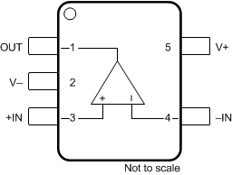
OPA187 OPA2187 OPA4187 DAPPER_Single_SOT23.gif
OPA187: D and DGK Packages
8-Pin SOIC and 8-pin VSSOP
Top View
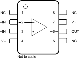
OPA187 OPA2187 OPA4187 DAPPER_Single_DIP.gif
NC denotes no internal connection.

Pin Functions: OPA187

PIN I/O DESCRIPTION
NAME DBV D and DGK
+IN 3 3 I Non-inverting input
–IN 4 2 I Inverting input
NC 1, 5, 8 No connection (can be left floating)
OUT 1 6 O Output signal
V+ 5 7 Positive (highest) supply voltage
V– 2 4 Negative (lowest) supply voltage
OPA2187: D and DGK Packages
8-Pin SOIC and 8-Pin VSSOP
Top View
OPA187 OPA2187 OPA4187 DAPPER_Dual_DIP.gif

Pin Functions: OPA2187

PIN I/O DESCRIPTION
NAME D and DGK
+IN A 3 I Non-inverting input, channel A
–IN A 2 I Inverting input, channel A
+IN B 5 I Non-inverting input, channel B
–IN B 6 I Inverting input, channel B
OUT A 1 O Output, channel A
OUT B 7 O Output, channel B
V+ 8 Positive (highest) supply voltage
V– 4 Negative (lowest) supply voltage
OPA4187: D and PW Packages
14-pin SOIC and 14-Pin TSSOP
Top View
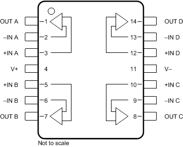
OPA187 OPA2187 OPA4187 DAPPER_Quad_DIP.gif
OPA4187: RUM Package (Preview)
16-pin WQFN
Top View

Pin Functions: OPA4187

PIN I/O DESCRIPTION
NAME D and PW RUM
+IN A 3 2 I Non-inverting input, channel A
–IN A 2 1 I Inverting input, channel A
+IN B 5 4 I Non-inverting input, channel B
–IN B 6 5 I Inverting input, channel B
+IN C 10 9 I Non-inverting input, channel C
–IN C 9 8 I Inverting input, channel C
+IN D 12 11 I Non-inverting input, channel D
–IN D 13 12 I Inverting input, channel D
OUT A 1 15 O Output, channel A
OUT B 7 6 O Output, channel B
OUT C 8 7 O Output, channel C
OUT D 14 14 O Output, channel D
V+ 4 3 Positive (highest) supply voltage
V– 11 10 Negative (lowest) supply voltage
NC 13, 16 No internal connection (can be left floating)