ZHCSFU2A December   2016  – January 2019 OPA4277-SP

PRODUCTION DATA.  

  1. 特性
  2. 应用
  3. 说明
    1.     Device Images
      1.      简化原理图
  4. 修订历史记录
  5. Pin Configuration and Functions
    1.     Pin Functions: CFP
    2.     Pin Functions: CDIP
    3. 5.1 Bare Die Information
      1.      Bond Pad Coordinates in Microns
  6. Specifications
    1. 6.1 Absolute Maximum Ratings
    2. 6.2 ESD Ratings
    3. 6.3 Recommended Operating Conditions
    4. 6.4 Thermal Information
    5. 6.5 Electrical Characteristics
    6. 6.6 Typical Characteristics
  7. Detailed Description
    1. 7.1 Overview
    2. 7.2 Functional Block Diagram
    3. 7.3 Feature Description
      1. 7.3.1 Input Protection
      2. 7.3.2 Input Bias Current Cancellation
    4. 7.4 Device Functional Modes
  8. Application and Implementation
    1. 8.1 Application Information
    2. 8.2 Typical Application
      1. 8.2.1 Design Requirements
      2. 8.2.2 Detailed Design Procedure
      3. 8.2.3 Application Curve
  9. Power Supply Recommendations
  10. 10Layout
    1. 10.1 Layout Guidelines
    2. 10.2 Layout Example
  11. 11器件和文档支持
    1. 11.1 接收文档更新通知
    2. 11.2 社区资源
    3. 11.3 商标
    4. 11.4 静电放电警告
    5. 11.5 术语表
  12. 12机械、封装和可订购信息

封装选项

机械数据 (封装 | 引脚)
散热焊盘机械数据 (封装 | 引脚)
订购信息

Typical Characteristics

At TJ = 25°C, VS = ±15 V, and RL = 2 kΩ, pre-irradiated (unless otherwise noted).
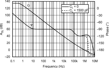
OPA4277-SP graph01_sbos771.gif
Figure 1. Open-Loop Gain/Phase vs Frequency
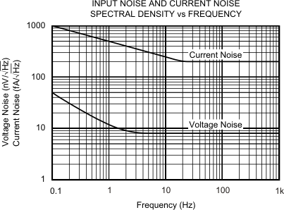
OPA4277-SP tc_input_current_noise_spec_density_bos079.gif
Figure 3. Input Noise and Current Noise Spectral Density vs Frequency
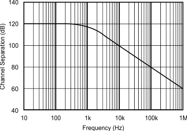
OPA4277-SP graph5_sbos771.gif
G = 1, measured channel A to D or B to C.
Other combinations yield similar or improved rejection.
Figure 5. Channel Separation vs Frequency
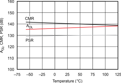
OPA4277-SP graph10_sbos714.gif
Figure 7. AOL, CMR, PSR vs Temperature
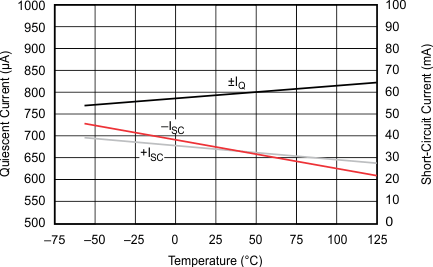
OPA4277-SP graph12_sbos714.gif
Figure 9. Quiescent Current and Short-Circuit Current vs Temperature
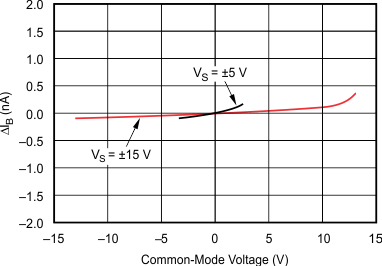
OPA4277-SP graph14_sbos771.gif
Curve shows normalized change in bias current with respect to VCM = 0 V. Typical IB may range from –0.5 nA to 0.5 nA at
VCM = 0 V.
Figure 11. Change in Input Bias Current vs Common-Mode Voltage
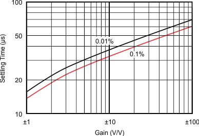
OPA4277-SP graph16_sbos714.gif
10-V step CL = 1500 pF
Figure 13. Settling Time vs Closed-Loop Gain
OPA4277-SP graph18_sbos714.gif
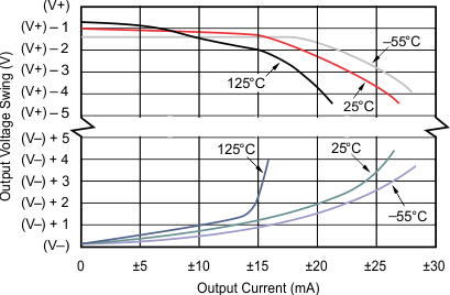
Figure 15. Output Voltage Swing vs Output Current
OPA4277-SP graph20_sbos771.gif
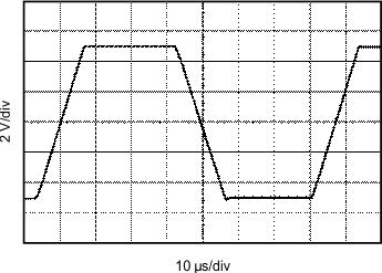
G = 1 CL = 1500 pF VS = ±15 V
Figure 17. Large-Signal Step Response
OPA4277-SP graph22_sbos771.gif
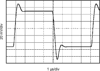
G = 1 CL = 1500 pF VS = ±15 V
Figure 19. Small-Signal Step Response
OPA4277-SP graph2_sbos714.gif
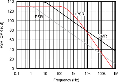
Figure 2. Power Supply and Common-Mode Rejection vs Frequency
OPA4277-SP graph04_sbos771.gif
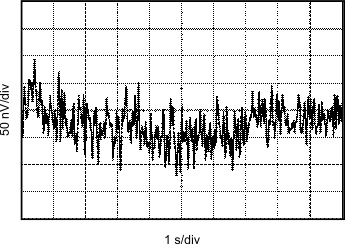
Noise signal is bandwidth limited to lie between 0.1 Hz and 10 Hz.
Figure 4. Input Noise Voltage vs Time
OPA4277-SP graph06_sbos771.gif
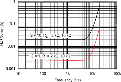
VOUT = 3.5 Vrms
Figure 6. Total Harmonic Distortion + Noise vs Frequency
OPA4277-SP graph11_sbos771.gif
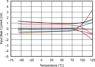
Curves represent typical production units.
Figure 8. Input Bias Current vs Temperature
OPA4277-SP graph13_sbos771.gif
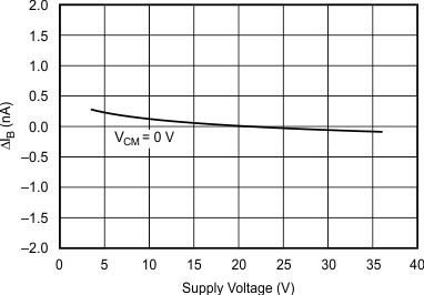
Curve shows normalized change in bias current with respect to VS = ±10 V (+20 V). Typical IB may range from –0.5 nA to 0.5 nA at VS = ±10 V.
Figure 10. Change in Input Bias Current vs Power Supply Voltage
OPA4277-SP graph15_sbos771.gif
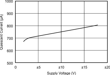
Per amplifier
Figure 12. Quiescent Current vs Supply Voltage
OPA4277-SP graph17_sbos771.gif
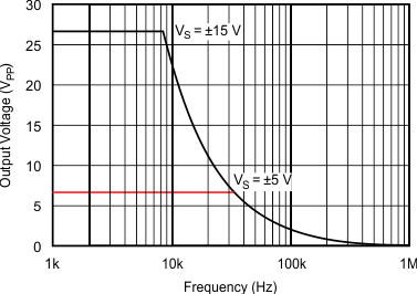
Figure 14. Maximum Output Voltage vs Frequency
OPA4277-SP graph19_sbos714.gif
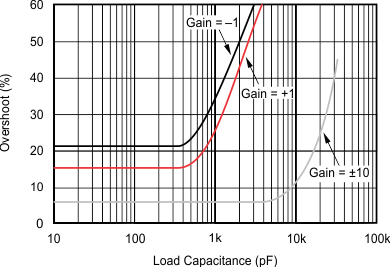
Figure 16. Small-Signal Overshoot vs Load Capacitance
OPA4277-SP graph21_sbos771.gif
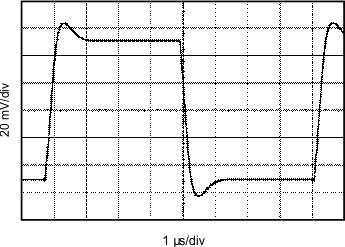
G = 1 CL = 0 pF VS = ±15 V
Figure 18. Small-Signal Step Response