ZHCS183G May 2011 – June 2015 OPA2314 , OPA314 , OPA4314
PRODUCTION DATA.
7 Detailed Description
7.1 Overview
The OPA314 is a family of low-power, rail-to-rail input and output operational amplifiers specifically designed for portable applications. These devices operate from 1.8 V to 5.5 V, are unity-gain stable, and suitable for a wide range of general-purpose applications. The class AB output stage is capable of driving ≤ 10-kΩ loads connected to any point between V+ and ground. The input common-mode voltage range includes both rails, and allows the OPA314 series to be used in virtually any single-supply application. Rail-to-rail input and output swing significantly increases dynamic range, especially in low-supply applications, and makes them ideal for driving sampling analog-to-digital converters (ADCs).
The OPA314 features 3-MHz bandwidth and 1.5-V/μs slew rate with only 150-μA supply current per channel, providing good AC performance at very low power consumption. DC applications are also well served with a very low input noise voltage of 14 nV/√Hz at 1 kHz, low input bias current (0.2 pA), and an input offset voltage of 0.5 mV (typical).
7.2 Functional Block Diagram

7.3 Feature Description
7.3.1 Operating Voltage
The OPA314 series operational amplifiers are fully specified and ensured for operation from 1.8 V to 5.5 V. In addition, many specifications apply from –40°C to 125°C. Parameters that vary significantly with operating voltages or temperature are shown in the Typical Characteristics graphs. Power-supply pins should be bypassed with 0.01-μF ceramic capacitors.
7.3.2 Rail-to-Rail Input
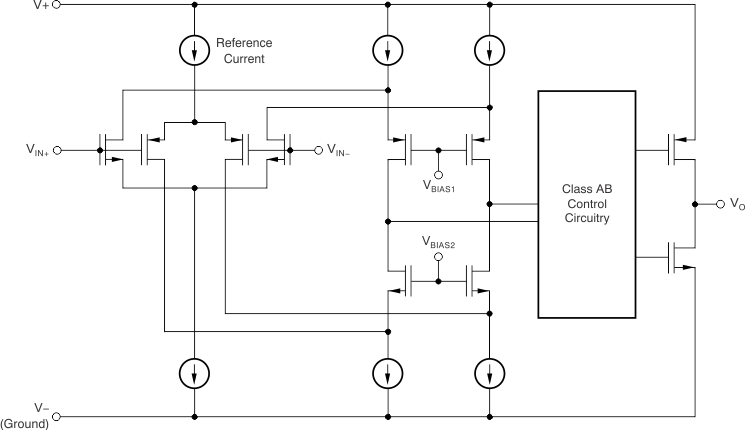
The input common-mode voltage range of the OPA314 series extends 200 mV beyond the supply rails. This performance is achieved with a complementary input stage: an N-channel input differential pair in parallel with a P-channel differential pair, as shown in Figure 33. The N-channel pair is active for input voltages close to the positive rail, typically (V+) – 1.3 V to 200 mV above the positive supply, while the P-channel pair is on for inputs from 200 mV below the negative supply to approximately (V+) – 1.3 V. There is a small transition region, typically (V+) – 1.4 V to (V+) – 1.2 V, in which both pairs are on. This 200-mV transition region can vary up to 300 mV with process variation. Thus, the transition region (both stages on) can range from (V+) – 1.7 V to (V+) – 1.5 V on the low end, up to (V+) – 1.1 V to (V+) – 0.9 V on the high end. Within this transition region, PSRR, CMRR, offset voltage, offset drift, and THD may be degraded compared to device operation outside this region.
 Figure 33. Simplified Schematic
7.3.3 Input and ESD Protection
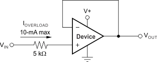
The OPA314 family incorporates internal electrostatic discharge (ESD) protection circuits on all pins. In the case of input and output pins, this protection primarily consists of current-steering diodes connected between the input and power-supply pins. These ESD protection diodes also provide in-circuit, input overdrive protection, as long as the current is limited to 10 mA as stated in the Absolute Maximum Ratings. Figure 34 shows how a series input resistor may be added to the driven input to limit the input current. The added resistor contributes thermal noise at the amplifier input and its value should be kept to a minimum in noise-sensitive applications.
 Figure 34. Input Current Protection
7.3.4 Common-Mode Rejection Ratio (CMRR)
CMRR for the OPA314 is specified in several ways so the best match for a given application may be used; see the Electrical Characteristics. First, the CMRR of the device in the common-mode range below the transition region [VCM < (V+) – 1.3 V] is given. This specification is the best indicator of the capability of the device when the application requires use of one of the differential input pairs. Second, the CMRR over the entire common-mode range is specified at (VCM = –0.2 V to 5.7 V). This last value includes the variations seen through the transition region (see Figure 7).
7.3.5 EMI Susceptibility and Input Filtering
Operational amplifiers vary with regard to the susceptibility of the device to electromagnetic interference (EMI). If conducted EMI enters the operational amplifier, the DC offset observed at the amplifier output may shift from its nominal value while EMI is present. This shift is a result of signal rectification associated with the internal semiconductor junctions. While all operational amplifier pin functions can be affected by EMI, the signal input pins are likely to be the most susceptible. The OPA314 operational amplifier family incorporate an internal input low-pass filter that reduces the amplifiers response to EMI. Both common-mode and differential mode filtering are provided by this filter. The filter is designed for a cutoff frequency of approximately 80 MHz (–3 dB), with a roll-off of 20 dB per decade.
Texas Instruments has developed the ability to accurately measure and quantify the immunity of an operational amplifier over a broad frequency spectrum extending from 10 MHz to 6 GHz. The EMI rejection ratio (EMIRR) metric allows operational amplifiers to be directly compared by the EMI immunity. Figure 32 illustrates the results of this testing on the OPAx314. Detailed information can also be found in the application report, EMI Rejection Ratio of Operational Amplifiers (SBOA128), available for download from www.ti.com.
7.3.6 Rail-to-Rail Output
Designed as a micro-power, low-noise operational amplifier, the OPA314 delivers a robust output drive capability. A class AB output stage with common-source transistors is used to achieve full rail-to-rail output swing capability. For resistive loads up to 10 kΩ, the output swings typically to within 5 mV of either supply rail regardless of the power-supply voltage applied. Different load conditions change the ability of the amplifier to swing close to the rails; refer to Figure 17.
7.3.7 Capacitive Load and Stability
The OPA314 is designed to be used in applications where driving a capacitive load is required. As with all operational amplifiers, there may be specific instances where the OPA314 can become unstable. The particular operational amplifiers circuit configuration, layout, gain, and output loading are some of the factors to consider when establishing whether or not an amplifier is stable in operation. An operational amplifier in the unity-gain (+1-V/V) buffer configuration that drives a capacitive load exhibits a greater tendency to be unstable than an amplifier operated at a higher noise gain. The capacitive load, in conjunction with the operational amplifier output resistance, creates a pole within the feedback loop that degrades the phase margin. The degradation of the phase margin increases as the capacitive loading increases. When operating in the unity-gain configuration, the OPA314 remains stable with a pure capacitive load up to approximately 1 nF. The equivalent series resistance (ESR) of some very large capacitors (CL greater than 1 μF) is sufficient to alter the phase characteristics in the feedback loop such that the amplifier remains stable. Increasing the amplifier closed-loop gain allows the amplifier to drive increasingly larger capacitance. This increased capability is evident when observing the overshoot response of the amplifier at higher voltage gains. See Figure 20.
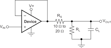
One technique for increasing the capacitive load drive capability of the amplifier operating in a unity-gain configuration is to insert a small resistor, typically 10 Ω to 20 Ω, in series with the output, as shown in Figure 35. This resistor significantly reduces the overshoot and ringing associated with large capacitive loads. One possible problem with this technique, however, is that a voltage divider is created with the added series resistor and any resistor connected in parallel with the capacitive load. The voltage divider introduces a gain error at the output that reduces the output swing.
 Figure 35. Improving Capacitive Load Drive
7.4 Device Functional Modes
The OPA2314 device is powered on when the supply is connected. The device can be operated as a single-supply operational amplifier or a dual-supply amplifier, depending on the application.