ZHCSRR8B October 2023 – April 2024 OPA2323 , OPA323 , OPA4323
PRODMIX
- 1
- 1 特性
- 2 应用
- 3 说明
- 4 Device Comparison Table
- 5 Pin Configuration and Functions
- 6 Specifications
-
7 Detailed Description
- 7.1 Overview
- 7.2 Functional Block Diagram
- 7.3
Feature Description
- 7.3.1 Operating Voltage
- 7.3.2 Rail-to-Rail Input
- 7.3.3 Rail-to-Rail Output
- 7.3.4 Common-Mode Rejection Ratio (CMRR)
- 7.3.5 Capacitive Load and Stability
- 7.3.6 Overload Recovery
- 7.3.7 EMI Rejection
- 7.3.8 ESD and Electrical Overstress
- 7.3.9 Input ESD Protection
- 7.3.10 Shutdown Function
- 7.3.11 Packages with an Exposed Thermal Pad
- 7.4 Device Functional Modes
- 8 Application and Implementation
- 9 Device and Documentation Support
- 10Revision History
- 11Mechanical, Packaging, and Orderable Information
封装选项
请参考 PDF 数据表获取器件具体的封装图。
机械数据 (封装 | 引脚)
- DYY|14
- PW|14
散热焊盘机械数据 (封装 | 引脚)
订购信息
7.3.5 Capacitive Load and Stability
The OPAx323 is designed for use in applications where driving a capacitive load is required. As with all operational amplifiers, there can be specific instances where the device can become unstable. The particular operational amplifier circuit configuration, layout, gain, and output loading are some of the factors to consider when establishing whether or not an amplifier is stable in operation.
An operational amplifier in the unity-gain (1V/V) buffer configuration that drives a capacitive load exhibits a greater tendency to be unstable than an amplifier operating at a higher noise gain. The capacitive load, in conjunction with the operational amplifier output resistance, creates a pole within the feedback loop that degrades the phase margin. The degradation of the phase margin increases when capacitive loading increases. When operating in the unity-gain configuration, the OPAx323 has a phase margin of 50° with 30pF of capacitive load. The device remains stable with pure capacitive loads up to approximately 75pF with acceptable phase margin of 35° and has no sustained oscillations up to 150pF. The equivalent series resistance (ESR) of some very large capacitors (greater than 1μF) is sometimes sufficient to alter the phase characteristics in the feedback loop such that the amplifier remains stable. Increasing the amplifier closed-loop gain allows the amplifier to drive increasingly larger capacitance. This increased capability is evident when measuring the overshoot response of the amplifier at higher voltage gains.
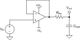
One technique for increasing the capacitive load drive capability of the amplifier operating in a unity-gain configuration is to insert a small resistor (typically 10Ω to 50Ω) in series with the output, as shown in Figure 7-3. This resistor significantly reduces the overshoot and ringing associated with large capacitive loads. This is usually the circuit configuration used in ADC driver application with Cload serving as a charge bucket for the ADC sampling capacitor.
 Figure 7-3 Improving
Capacitive Load Drive