SBOS432G August 2008 – August 2016 OPA2330 , OPA330 , OPA4330
PRODUCTION DATA.
- 1 Features
- 2 Applications
- 3 Description
- 4 Revision History
- 5 Device Comparison Table
- 6 Pin Configurations and Functions
- 7 Specifications
- 8 Detailed Description
- 9 Application and Implementation
- 10Power Supply Recommendations
- 11Layout
- 12Device and Documentation Support
- 13Mechanical, Packaging, and Orderable Information
封装选项
请参考 PDF 数据表获取器件具体的封装图。
机械数据 (封装 | 引脚)
- D|14
- RGY|14
- PW|14
散热焊盘机械数据 (封装 | 引脚)
- RGY|14
订购信息
6 Pin Configurations and Functions
OPA330: D Package
8-Pin SOIC
Top View
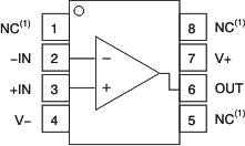
1. NC denotes no internal connection.
OPA330: DBV Package
5-Pin SOT-23
Top View
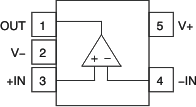
OPA330: DCK Package
5-Pin SC70
Top View
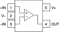
OPA330: YFF Package
5-Pin DSBGA
Top View
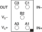
Pin Functions: OPA330
OPA2330: D and DGK Packages
8-Pin SOIC and 8-Pin VSSOP
Top View
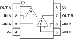
OPA2330: DRB Package
8-Pin SON
Top View
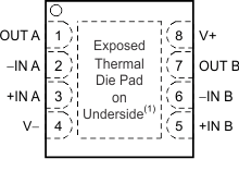
1. Connect thermal die pad to V–.
Pin Functions: OPA2330
| PIN | I/O | DESCRIPTION | ||
|---|---|---|---|---|
| NAME | SOIC, VSSOP |
SON | ||
| –IN A | 2 | 2 | I | Negative (inverting) input signal, channel A |
| +IN A | 3 | 3 | I | Positive (noninverting) input signal, channel A |
| –IN B | 6 | 6 | I | Negative (inverting) input signal, channel B |
| +IN B | 5 | 5 | I | Positive (noninverting) input signal, channel B |
| OUT A | 1 | 1 | O | Output channel A |
| OUT B | 7 | 7 | O | Output channel B |
| V– | 4 | 4 | — | Negative (lowest) power supply |
| V+ | 8 | 8 | — | Positive (highest) power supply |
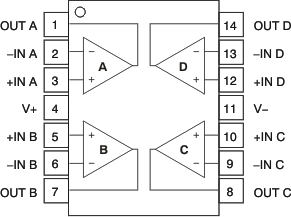
OPA4330: D Package
14-Pin SOIC
Top View
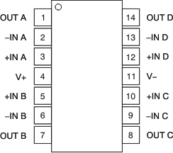
OPA4330: PW Package
14-Pin TSSOP
Top View
OPA4330: RGY Package
14-Pin VQFN
Top View
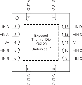
1. Connect thermal die pad to V–.
Pin Functions: OPA4330
| PIN | I/O | DESCRIPTION | |||
|---|---|---|---|---|---|
| NAME | SOIC | TSSOP | VQFN | ||
| –IN A | 2 | 2 | 2 | I | Negative (inverting) input signal, channel A |
| +IN A | 3 | 3 | 3 | I | Positive (noninverting) input signal, channel A |
| –IN B | 6 | 6 | 6 | I | Negative (inverting) input signal, channel B |
| +IN B | 5 | 5 | 5 | I | Positive (noninverting) input signal, channel B |
| –IN C | 9 | 9 | 9 | I | Negative (inverting) input signal, channel C |
| +IN C | 10 | 10 | 10 | I | Positive (noninverting) input signal, channel C |
| –IN D | 13 | 13 | 13 | I | Negative (inverting) input signal, channel D |
| +IN D | 12 | 12 | 12 | I | Positive (noninverting) input signal, channel D |
| OUT A | 1 | 1 | 1 | O | Output channel A |
| OUT B | 7 | 7 | 7 | O | Output channel B |
| OUT C | 8 | 8 | 8 | O | Output channel C |
| OUT D | 14 | 14 | 14 | O | Output channel D |
| V– | 11 | 11 | 11 | — | Negative (lowest) power supply |
| V+ | 4 | 4 | 4 | — | Positive (highest) power supply |