SBOS073C September 1997 – August 2016 OPA2340 , OPA340 , OPA4340
PRODUCTION DATA.
- 1 Features
- 2 Applications
- 3 Description
- 4 Revision History
- 5 Pin Configuration and Functions
- 6 Specifications
- 7 Detailed Description
- 8 Application and Implementation
- 9 Power Supply Recommendations
- 10Layout
- 11Device and Documentation Support
- 12Mechanical, Packaging, and Orderable Information
8 Application and Implementation
NOTE
Information in the following applications sections is not part of the TI component specification, and TI does not warrant its accuracy or completeness. TI’s customers are responsible for determining suitability of components for their purposes. Customers should validate and test their design implementation to confirm system functionality.
8.1 Application Information
The OPAx340 amplifier is a single-supply, CMOS operational amplifier with 5.5-MHz unity-gain bandwidth and supply current of 950 µA. Its performance is optimized for low-voltage (2.7 V to 5.5 V), single-supply applications, with its input common-mode voltage linear range extending 300 mV beyond the rails and the output voltage swing within 5 mV of either rail. The OPAx340 series features wide bandwidth and unity-gain stability with rail-to-rail input and output for increased dynamic range. Power-supply pins must be bypassed with 0.01-µF ceramic capacitors.
8.2 Typical Applications
8.2.1 Single-Pole, Low-Pass Filter
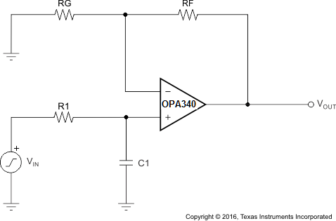
Figure 29 shows the OPA340 in a typical noninverting application with the input signal bandwidth limited by the input lowpass filter.
 Figure 29. Single-Pole, Low-Pass Filter
Equation 1 through Equation 2 show calculations for corner frequency and gain:


8.2.1.1 Design Requirements
When receiving low-level signals, limiting the bandwidth of the incoming signals into the system is often required. The simplest way to establish this limited bandwidth is to place an RC filter at the noninverting terminal of the amplifier, as shown in Figure 29. If a steeper attenuation level is required, a two-pole or higher-order filter may be used.
8.2.1.2 Detailed Design Procedure
The design goals for this circuit include these parameters:
- A noninverting gain of 10 V/V (20 dB)
- Design a single-pole response circuit with –3-dB rolloff at 15.9 kHz and 159 Hz
- Modify the design to increase attenuation level to –40 dB/decade (Sallen-Key Filter)
Use these design values:
- C1 = 0 nF, 10 nF, 1 µF
- R1 = 1 kΩ
- RG = 10 kΩ
- RF = 90 kΩ
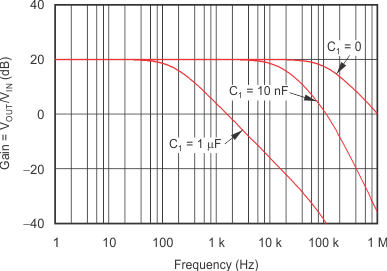
Figure 30 shows how the output voltage of OPA340 changes over frequency depending on the value of C1 with a constant R1 of 1 kΩ. Without any filtering of the input signal (C1 = 0), the –3-dB effective bandwidth is a function of the OPA340 unity-gain bandwidth and closed-loop gain, f(–3dB) = UGBW/ACL, where ACL is closed-loop gain and UGBW denotes unity-gain bandwidth. Thus, for a closed-loop gain = 10, f(–3dB) = 1 MHz/10 =100 kHz; see Figure 30.
To further limit the output bandwidth, an appropriate choice of C1 must be made: for C1 = 10 nF,  = 15.9 kHz.
To further limit the bandwidth, a larger C1 must be used: choosing C1 = 1 µF,
 = 159 Hz (see Figure 30).
8.2.1.3 Application Curve
 Figure 30. OPA340 Single-Pole AC Gain vs Frequency Response
8.2.2 Two-Pole, Low-Pass Filter
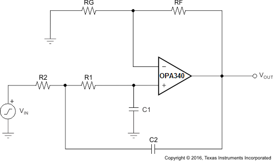
If even more attenuation is required, a multiple pole filter is required. The Sallen-Key filter may be used for this task, as shown in Figure 31. For best results, the amplifier must have effective bandwidth that is at least 10 times higher than the filter cutoff frequency. Failure to follow this guideline results in a phase shift of the amplifier, which in turn leads to lower precision of the filter bandwidth. Additionally, to minimize the loading effect between multiple RC pairs on overall the filter cutoff frequency, choose R = 10 × R1 and C2 = C1/10; see Figure 32.
 Figure 31. Two-Pole, Lowpass Filter
Equation 3 through Equation 5 show calculations for corner frequency and gain:


8.2.2.1 Detailed Design Procedure
Use these design values:
- C1 = 10 nF and C2 = 1 nF
- R1 = 1 kΩ and R2= 10 kΩ
- RG = 10 kΩ
- RF = 90 kΩ
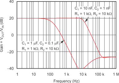
Figure 32 shows the Sallen-Key filter second-order response for different RC values: for R and C values above,  = 15.9 kHz.
To further limit the bandwidth, a larger RC value must be used: increasing C values 100 times, such as
C1 = 1 µF and C2 = 0.1 µF, with unchanged resistors, results in the second-order rolloff at  = 159 Hz. See Figure 32.
8.2.2.2 Application Curve
 Figure 32. OPA340 Two-Pole, Lowpass Sallen-Key AC Gain vs Frequency Response