ZHCSI77F June   2009  – May 2018 OPA2354A-Q1 , OPA354A-Q1 , OPA4354-Q1

PRODUCTION DATA.  

  1. 特性
  2. 应用
  3. 说明
    1.     简化原理图
  4. 修订历史记录
  5. Pin Configuration and Functions
    1.     Pin Functions: OPA354A-Q1
    2.     Pin Functions: OPA2354A-Q1
    3.     Pin Functions: OPA4354-Q1
  6. Specifications
    1. 6.1 Absolute Maximum Ratings
    2. 6.2 ESD Ratings
    3. 6.3 Recommended Operating Conditions
    4. 6.4 Thermal Information: OPA354A-Q1
    5. 6.5 Thermal Information: OPA2354A-Q1
    6. 6.6 Thermal Information: OPA4354A-Q1
    7. 6.7 Electrical Characteristics
    8. 6.8 Typical Characteristics
  7. Detailed Description
    1. 7.1 Overview
    2. 7.2 Functional Block Diagram
    3. 7.3 Feature Description
      1. 7.3.1 Operating Voltage
      2. 7.3.2 Rail-to-Rail Input
      3. 7.3.3 Rail-to-Rail Output
      4. 7.3.4 Output Drive
      5. 7.3.5 Video
      6. 7.3.6 Driving Analog-to-Digital Converters
      7. 7.3.7 Capacitive Load and Stability
      8. 7.3.8 Wideband Transimpedance Amplifier
    4. 7.4 Device Functional Modes
  8. Application and Implementation
    1. 8.1 Application Information
    2. 8.2 Typical Applications
      1. 8.2.1 Transimpedance Amplifier
        1. 8.2.1.1 Design Requirements
        2. 8.2.1.2 Detailed Design Procedure
          1. 8.2.1.2.1 Optimizing The Transimpedance Circuit
        3. 8.2.1.3 Application Curve
      2. 8.2.2 High-Impedance Sensor Interface
      3. 8.2.3 Driving ADCs
      4. 8.2.4 Active Filter
  9. Power Supply Recommendations
    1. 9.1 Power Dissipation
  10. 10Layout
    1. 10.1 Layout Guidelines
    2. 10.2 Layout Example
  11. 11器件和文档支持
    1. 11.1 文档支持
      1. 11.1.1 相关文档
    2. 11.2 相关链接
    3. 11.3 接收文档更新通知
    4. 11.4 社区资源
    5. 11.5 商标
    6. 11.6 静电放电警告
    7. 11.7 术语表
  12. 12机械、封装和可订购信息

封装选项

机械数据 (封装 | 引脚)
散热焊盘机械数据 (封装 | 引脚)
订购信息

High-Impedance Sensor Interface

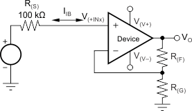
Many sensors have high source impedances that may range up to 10 MΩ, or even higher. The output signal of sensors often must be amplified or otherwise conditioned by an amplifier. The input bias current of this amplifier can load the sensor output and cause a voltage drop across the source resistance, as shown in Figure 40, where (V(+INx) = VS – I(BIAS) × R(S)). The last term, I(BIAS) × R(S), shows the voltage drop across R(S). To prevent errors introduced to the system as a result of this voltage, use an op amp with low input bias current and high-impedance sensors. This low current keeps the error contribution by I(BIAS) × R(S) less than the input voltage noise of the amplifier, so that the amplifier does not become the dominant noise factor. The OPAx354-Q1 family of devices series of op amps feature low input bias current (typically 200 fA), and are therefore designed for such applications.
OPA354A-Q1 OPA2354A-Q1 OPA4354-Q1 ai_noise_ibias_sbos492.gifFigure 40. Noise as a Result of I(BIAS)